Manufacturing process of subminiature inductor

A manufacturing process, ultra-small technology, applied in the field of manufacturing ultra-small inductors, can solve the problems that cannot completely replace the wire-wound chip inductors, poor inductance performance, large inductance thickness, etc., to facilitate the rapid production of machine automation, The effect of improving the qualified rate of products and reducing the amount of wire rod

Inactive Publication Date: 2011-11-02
广东麦新电子科技有限公司
View PDF7 Cites 1 Cited by
  • Summary
  • Abstract
  • Description
  • Claims
  • Application Information

AI Technical Summary

Problems solved by technology

The advantage of this kind of inductor is that the production process is simple, the electrical performance is excellent (the inductance value L and the quality factor Q are high), it is suitable for passing large currents, it has high reliability, and it is more suitable for high-frequency use. The disadvantage is that it is affected by the physical size and manufacturing of the magnetic core. Process limitations, limited size miniaturization
At present, products with a size of 2.5×2.0mm have been commercialized, and further miniaturization is difficult
For example, the patent No. CN200810142161.9 provides "an inductor and its manufacturing method". Combining and insulating dielectric layer, although the inductance is reduced to a certain extent, which is beneficial to expand the use range of the inductor, but its structure is complex, the thickness of the inductor is large, and the inductance performance is poor, so it cannot meet the technical requirements of limited space.
[0004] The multilayer chip inductor is alternately printed, laminated and sintered with ferrite paste and conductive paste to form a closed magnetic circuit. It adopts thick film multi-layer printing technology and laminated production process to achieve ultra-small surface mount , has the characteristics of miniaturization, closed magnetic circuit structure, easy mounting, and integration, but due to reasons such as precision, power, and price, it still cannot completely replace wire-wound chip inductors
For example, the application number CN200980116755.5 discloses "multilayer inductor and its manufacturing method", which has a plurality of magnetic layers including Ni-Zn-Cu ferrite, and a plurality of conductive layers forming coils through the magnetic layer. A body layer, and a cuboid-shaped laminate of a nonmagnetic layer formed adjacent to a plurality of magnetic layers and including at least one Ti-Ni-Cu-Mn-Zr based dielectric, and a laminate provided on the laminate At least one pair of external electrodes at the end and conductively connected to the end of the above-mentioned coil have good DC superposition characteristics, but this inductor is composed of multiple magnetic layers, conductive layers, etc., so the volume and thickness are large, and the process Complicated, cost-increased, unsuitable for technical applications with limited space

Method used


Image

  • Manufacturing process of subminiature inductor
  • Manufacturing process of subminiature inductor
  • Manufacturing process of subminiature inductor

Examples


Embodiment Construction

[0016] The present invention will be described in further detail below in conjunction with the accompanying drawings.

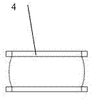
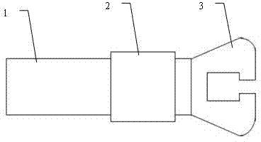
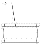
[0017] as attached figure 1 , attached figure 2 As shown, a manufacturing process of ultra-small inductors includes the I-shaped magnetic core electroplating process, winding process, DC welding process, and magnetic glue coating process. First, a metal layer is electroplated on the two bottom surfaces of the I-shaped magnetic core as Electrodes, and then put the I-shaped magnetic core on the fixture of the spot welding machine for winding, and then use the spot welding machine DC welding process that is convenient for automatic operation to carry out spot welding connection, and finally cover the inductance coil with magnetic epoxy resin glue surface layer.

[0018] The electroplating process of the I-shaped magnetic core is to electroplate a metal layer on the two bottom surfaces of the I-shaped magnetic core (4) as electrodes, so as to compress the heig...


PUM


Abstract

The invention discloses a manufacturing process of a subminiature inductor. The process comprises an I-shaped magnetic core electroplating process, a coiling process, a direct current welding process and a magnetic glue cladding process and comprises the following specific steps: at the two bottom surfaces of an I-shaped magnetic core, respectively electroplating one metal layer at the two bottom surfaces of an I-shaped magnetic core to serve as an electrode; then coiling the I-shaped magnetic core on a clamp of a spot welder; carrying out spot wielding connection by use of a spot welder direct current welding process which is convenient for automation operation; and finally, cladding magnetic epoxy resin flue on the surface layer of an inductive coil. According to the invention, a novel and advanced manufacturing process is adopted, the produced inductor is ultrathin and subminiature, and the property of the inductor is improved; and because a direct current welding process is used, the qualification rate of the product is improved, multiple working procedures are omitted, the product cost is greatly reduced, and the height size of the product can be well controlled so as to facilitate the rapid automatic production of a machine.

Description

technical field [0001] The invention relates to a manufacturing process of an inductor, in particular to a manufacturing process of an ultra-small inductor. Background technique [0002] The main functions of inductors are to screen signals, filter noise, stabilize current and control electromagnetic wave interference. Inductors can be divided into two categories: plug-in inductors and chip inductors. Due to the strong demand of downstream industries, chip inductors have huge room for development. Chip inductors can be divided into four categories: multilayer chip inductors, wire wound chip inductors, braided chip inductors and film chip inductors. Among them, multilayer chip inductors and wire wound chip inductors are the two most commonly used types of chip inductors. [0003] Wire-wound chip inductors usually use tiny I-shaped magnetic cores, which are made by winding, welding, electrode forming, and then plastic packaging. The advantage of this kind of inductor is th...

Claims


Application Information

Patent Timeline
Patent Type & Authority Applications(China)
IPC IPC(8): H01F41/00H01F17/00H01F37/00
Inventor 张国光
Owner 广东麦新电子科技有限公司
Why Eureka
Try Eureka