Method for inducing amorphous silicon film with tin to be crystallized into polycrystalline silicon film

A technology of amorphous silicon thin film and polycrystalline silicon thin film, which is applied in semiconductor/solid-state device manufacturing, electrical components, circuits, etc., can solve the problems of difficult application and high crystallization temperature, and achieve low cost, simple process structure and convenient operation Effect

Inactive Publication Date: 2013-04-03
SHANGHAI UNIV
View PDF4 Cites 0 Cited by
  • Summary
  • Abstract
  • Description
  • Claims
  • Application Information

AI Technical Summary

Problems solved by technology

[0007] The crystallization temperature of (SPC) is too high, and it takes more than 20 hours to crystallize amorphous silicon into polycrystalline silicon at a temperature above 600 ° C. Therefore, it is difficult to be applied on cheap glass substrates. The base material is quartz or single crystal silicon.

Method used


Image

  • Method for inducing amorphous silicon film with tin to be crystallized into polycrystalline silicon film
  • Method for inducing amorphous silicon film with tin to be crystallized into polycrystalline silicon film
  • Method for inducing amorphous silicon film with tin to be crystallized into polycrystalline silicon film

Examples


Embodiment

[0031] The process and steps in the embodiment of the present invention are as follows:

[0032] (1) Cut the ordinary glass substrate into 1cm×1cm size, wash off the surface dirt with detergent, and then ultrasonically clean it in acetone and deionized water for 15 minutes, then put it in an oven for drying;

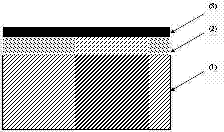
[0033] (2) Deposit a layer of amorphous silicon (a-Si:H) film on a glass substrate by plasma enhanced chemical deposition (PECVD) with a thickness of about 200nm. The substrate temperature during deposition is 200°C and the deposition pressure is 10 -5 Pa, gas glow pressure range 50Pa-250Pa, RF power supply 13.56MHz, gas source is 100% pure silane (SiH 4 ), hydrogen used as dilute silane (H 2 ) purity is 5N;

[0034] (3) Soak the grown amorphous silicon sample in 1% hydrofluoric acid (HF) for 10 seconds, remove the oxide layer on the surface of the amorphous silicon film, take it out, rinse with deionized water, and then nitrogen (N 2 ) to dry, and then put it into a ...


PUM

PropertyMeasurementUnit
thicknessaaaaaaaaaa
particle sizeaaaaaaaaaa
thicknessaaaaaaaaaa

Abstract

The invention relates to a method for preparing a polycrystalline silicon thin film, in particular to a method for inducing an amorphous silicon thin film with tin to be crystallized into a polycrystalline silicon thin film at a low temperature. according to the main technical scheme of the invention, the method comprises the following steps of: 1, carrying out ultrasonic cleaning on a glass substrate by using acetone and deionized water respectively to clean the glass substrate; 2, growing a layer of amorphous silicon (a-Si:H) thin film on the glass substrate by using a plasma enhanced chemical vapor deposition method (PECVD), wherein the temperature of the substrate is about 200 DEG C, and the thickness of the thin film is 200nm-300nm during deposition; 3, growing a layer of metal tin (Sn) thin film with the thickness of 10nm-20nm on the amorphous silicon thin film by using a physical vapor deposition method so as to obtain a substrate / (a-Si:H) / Sn structure; 4, arranging the substrate / (a-Si:H) / Sn in a heat treatment furnace in a laminated manner, and carrying out heat treatment for more than 1 hour at the temperature of 450 DEG C, then cooling naturally, where nitrogen (N2) is introduced and used as a protection gas during the whole annealing process; and 5, removing the remained metal tin on the surface with concentrated hydrochloric acid with the concentration of 37.5% to finally obtain the polycrystalline silicon thin film which is crystallized under the induction of tin, wherein the particle size is about 70-200nm. The method is applicable to the fields of thin-film field effect transistors and solar cells.

Description

technical field [0001] The invention relates to a method for preparing a polysilicon thin film, specifically a method for inducing the crystallization of an amorphous silicon thin film into a polysilicon thin film by using metal tin at low temperature. Background technique [0002] Compared with the carrier mobility of amorphous silicon film (0.3-1.0cm 2 / (V·s)) compared with polysilicon thin film carrier mobility is 8 to 9 times higher, and thus widely used in flat panel displays, image sensors and solar cells. [0003] In the past few years, many technical methods for preparing polysilicon on glass substrates have been proposed, such as rapid thermal annealing (RTA), excimer laser crystallization (ELA), solid phase crystallization (SPC) and metal-induced crystallization. method (MIC), etc. [0004] The rapid annealing (RTA) process consists of three stages: heating stage, stabilization stage and cooling stage. When the power of the annealing furnace is turned on, the te...

Claims


Application Information

Patent Timeline
Patent Type & Authority Patents(China)
IPC IPC(8): H01L21/20H01L21/02
Inventor 孙杰史伟民
Owner SHANGHAI UNIV
Why Eureka
Try Eureka