A manufacturing method of an optical fiber preform with a uniform optical waveguide axis
An optical fiber preform and manufacturing method technology, which is applied to glass fiber products, manufacturing tools, glass manufacturing equipment and other directions, can solve the problems of low optical fiber uniformity and low utilization rate, etc., to improve the drawing strength characteristics, improve production efficiency, high purity effect
- Summary
- Abstract
- Description
- Claims
- Application Information
AI Technical Summary
Problems solved by technology
Method used
Image
Examples
Embodiment 1
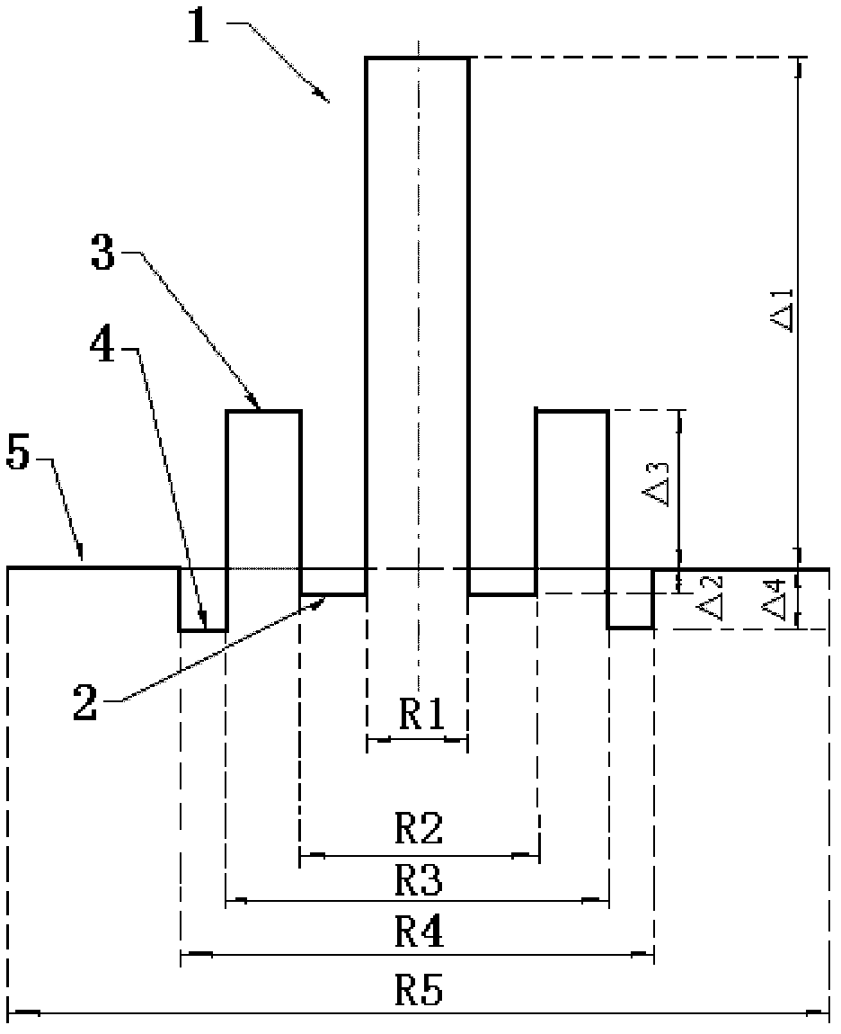
[0064] figure 1 Shown is a G655 optical fiber waveguide refractive index distribution curve in Example 1 of the present invention, the optical fiber section adopts a five-layer design, and its structural parameters ⊿ i (%) and R i (um) are: layer 1, 0.52, 5.2; layer 2, -0.08, 10.2; layer 3, 0.29, 15; layer 4, -0.08, 20; layer 5, 0, 125. In order to reflect the geometric characteristics of the fiber waveguide structure and facilitate process calculation and control, normalization is performed according to the diameter (R1) of layer 1, that is, the normalized diameter R of each layer i ’=R i / R 1 (i=1~5), get the normalized size: 1, 1.96, 2.88, 3.58, 24.04.
[0065] image 3 It is a schematic process flow diagram of the present invention. according to image 3 The G655 optical fiber of Example 1 of the present invention was prepared. Figure 4 and Figure 5 It is the process of using the MCVD method to make a mandrel in Example 1 of the present invention. exist Fig...
Embodiment 2
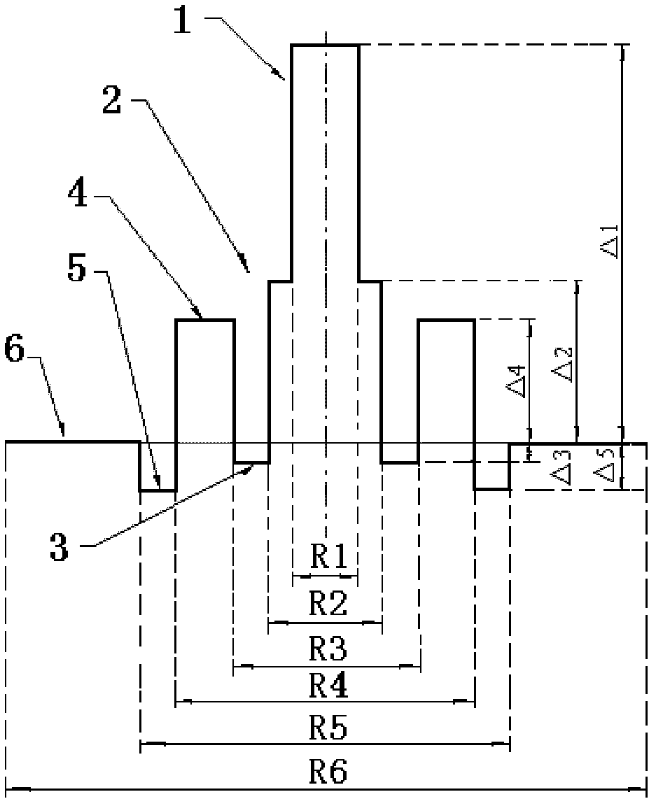
[0069] figure 2 Shown is a G656 optical fiber waveguide refractive index distribution curve in Example 2 of the present invention, the optical fiber section adopts a six-layer design, and its structural parameters ⊿ i (%) and R i (um) are: layer 1, 0.46, 5.8; layer 2, 0.25, 6.8; layer 3, -0.09, 11.8; layer 4, 0.25, 16.8; layer 5, -0.16, 19.8; layer 6, 0, 125. In order to reflect the geometric characteristics of the fiber waveguide structure and facilitate process calculation and control, normalization is performed according to the diameter (R1) of layer 1, that is, the normalized diameter R of each layer i ’=R i / R 1 (i=1~6), get the normalized size: 1, 1.17, 2.03, 2.9, 3.41, 21.55.
[0070] image 3 It is a schematic process flow diagram of the present invention. according to figure 2 The G656 optical fiber of Example 2 of the present invention was prepared. Figure 4 and Figure 5 It is the process of using the MCVD method to make the mandrel in Example 2 of th...
PUM
 Abstract
Description
Claims
Application Information
 - R&D
- Intellectual Property
- Life Sciences
- Materials
- Tech Scout
- Unparalleled Data Quality
- Higher Quality Content
- 60% Fewer Hallucinations
Browse by: Latest US Patents, China's latest patents, Technical Efficacy Thesaurus, Application Domain, Technology Topic, Popular Technical Reports.
© 2025 PatSnap. All rights reserved.Legal|Privacy policy|Modern Slavery Act Transparency Statement|Sitemap|About US| Contact US: help@patsnap.com


