Double sensitive layer gas sensor with nanofiber and particle adhesion layer and preparation method
A gas sensor and nanofiber layer technology, which is applied in coatings, instruments, scientific instruments, etc., can solve the problems of reducing sensitivity, fiber shrinkage, loss, etc., achieves improved sensitivity and response recovery, is easy to mass produce, and has a simple manufacturing process Effect
- Summary
- Abstract
- Description
- Claims
- Application Information
AI Technical Summary
Problems solved by technology
Method used
Image
Examples
Embodiment 1
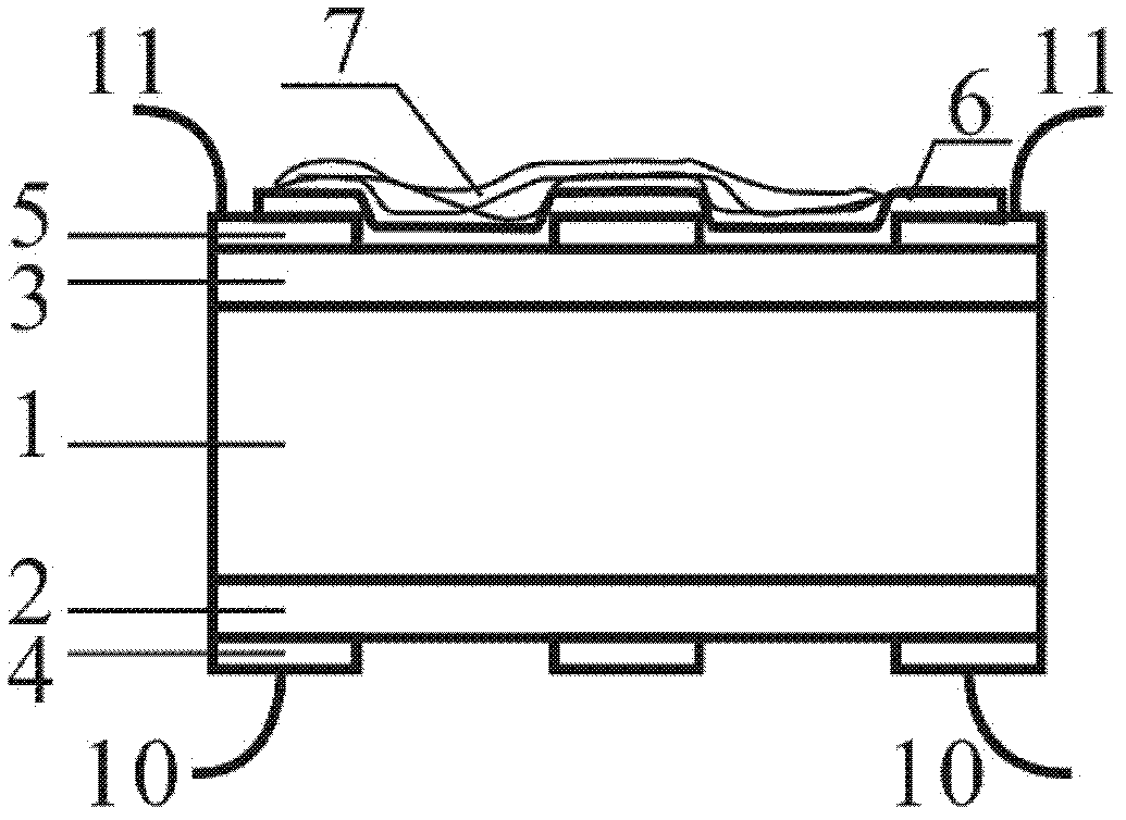
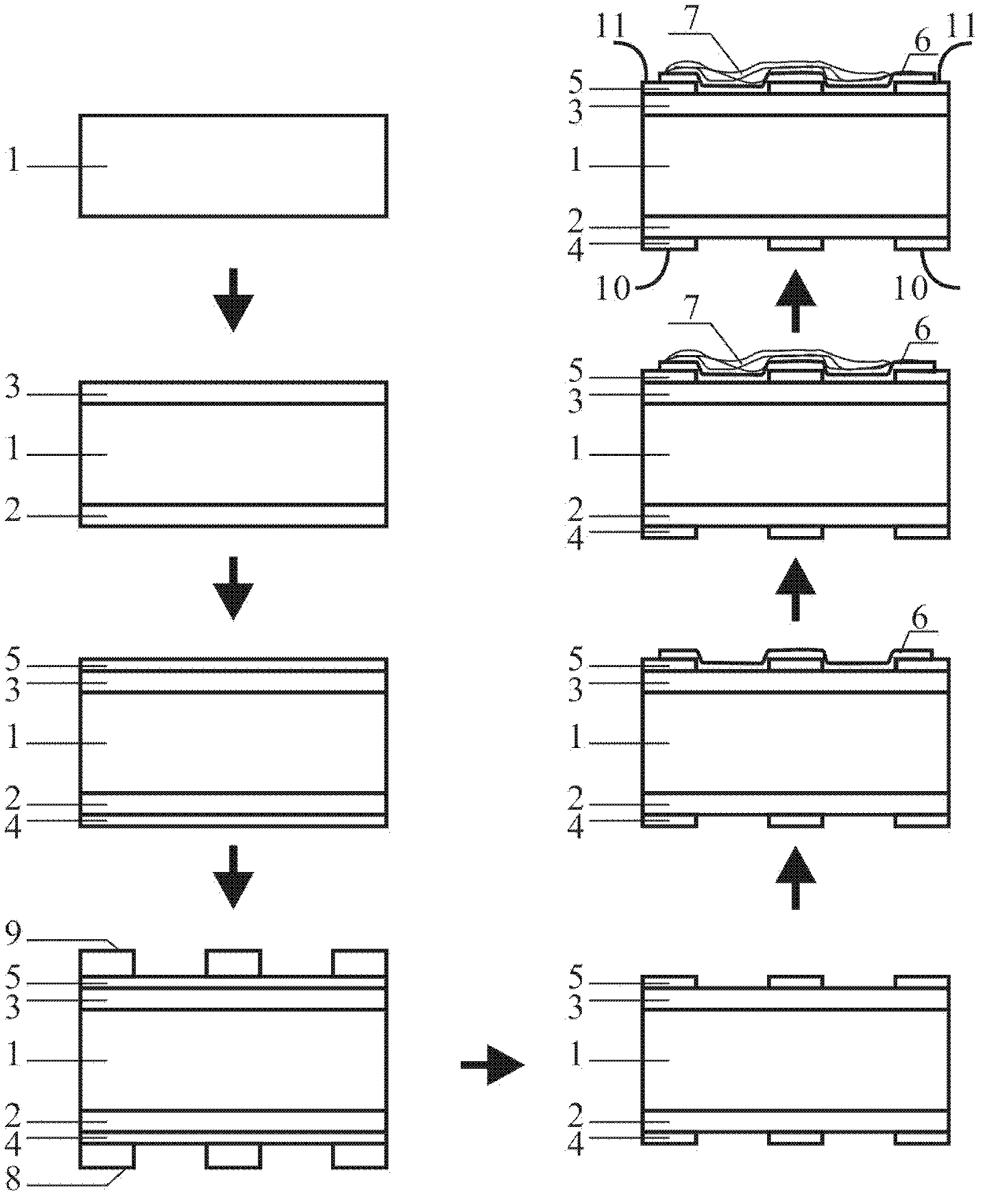
[0035] 1. On a double-sided polished oriented silicon wafer 1 (thickness 0.4mm), deposit SiO with a thickness of 400nm on both sides of the silicon wafer 1 at 300°C by PECVD method 2 Lower insulating layer 2 and upper insulating layer 3;
[0036] 2. Using the Pt target as the sputtering source, under the conditions of power 120W, Ar gas ambient pressure 1Pa, and substrate 300°C, sputter for 2 hours to obtain a Pt layer with a thickness of 100nm on the lower surface of the lower insulating layer 2 as a heating electrode layer;
[0037] 3. Using the Pt target as the sputtering source, under the conditions of 120W power, Ar gas ambient pressure 1Pa, and substrate 300°C, sputter for 2h to obtain a Pt layer with a thickness of 100nm on the upper surface of the upper insulating layer 3 as the signal electrode layer ;
[0038] 4. Apply GP18 photoresist (Chengdu Spectrum Optoelectronics Technology Co., Ltd.) on the heating electrode layer, spin the glue at 2400 rpm, and pre-bake at 60...
Embodiment 2
[0048] 1. Same as example 1;
[0049] 2. Same as example 1;
[0050] 3. Same as example 1;
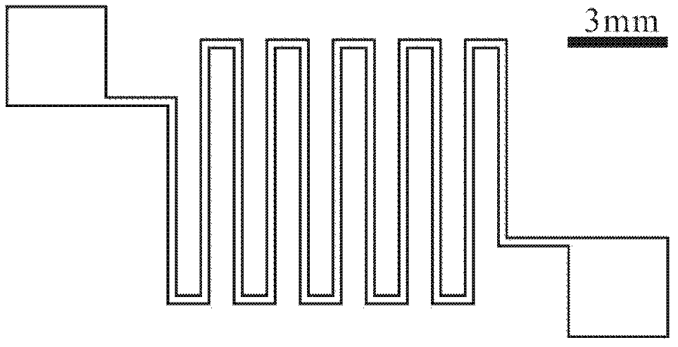
[0051] 4. Apply GP18 photoresist on the heating electrode layer, spin the glue at 2400 rpm, and pre-bake at 60°C for 30 minutes. image 3 The mask plate with the structure shown is exposed to ultraviolet light for 15s, then developed and baked at 150°C for 1h, so that the unexposed photoresist forms a heating electrode protective layer 8 on the heating electrode layer;
[0052] 5. Same as example 1;
[0053] 6. Same as Example 1, the obtained annular heating electrode 4 has a width of 0.25mm, a length of about 160mm, and a resistance value of about 21Ω;
[0054] 7. Same as example 1;
[0055] 8. Deposition of TiO on the signal electrode 5 by magnetron sputtering 2 Particle adhesion layer 6, using TiO 2 The target is used as the source, under the conditions of power 110W, Ar gas ambient pressure 1Pa, and substrate 100°C, sputter for 30min to obtain TiO with a thickness of 100nm 2...
PUM
| Property | Measurement | Unit |
|---|---|---|
| thickness | aaaaa | aaaaa |
| thickness | aaaaa | aaaaa |
| thickness | aaaaa | aaaaa |
Abstract
Description
Claims
Application Information


