Manufacturing method for cavity of full silica-based microfluidic device

The technology of a microfluidic device and manufacturing method, which is applied in the field of cavity manufacturing, can solve the problems of large chip area occupation, unfavorable reliability, complex process, etc., and achieve the effects of improving reliability, saving chip area, and reducing process difficulty

Active Publication Date: 2012-01-18
ADVANCED SEMICON MFG CO LTD
View PDF12 Cites 9 Cited by
  • Summary
  • Abstract
  • Description
  • Claims
  • Application Information

AI Technical Summary

Problems solved by technology

This kind of method involves bonding and bonding process, the chip area occupies a large area, the cost is high, the process is relatively complica

Method used


Image

  • Manufacturing method for cavity of full silica-based microfluidic device
  • Manufacturing method for cavity of full silica-based microfluidic device
  • Manufacturing method for cavity of full silica-based microfluidic device

Examples


Embodiment Construction

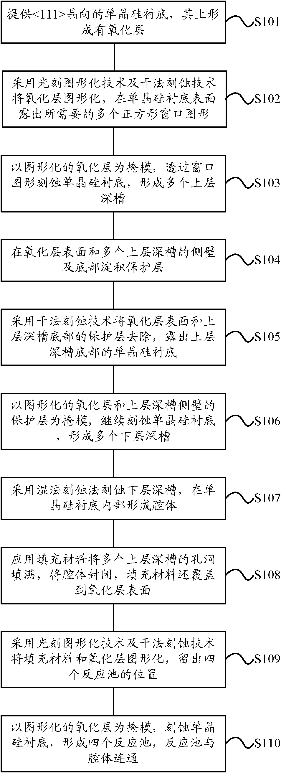
[0037] The present invention will be further described below in conjunction with specific embodiment and accompanying drawing, set forth more details in the following description so as to fully understand the present invention, but the present invention can obviously be implemented in a variety of other ways different from this description, Those skilled in the art can make similar promotions and deductions based on actual application situations without violating the connotation of the present invention, so the content of this specific embodiment should not limit the protection scope of the present invention.

[0038] figure 1 It is a flowchart of a method for manufacturing a cavity of an all-silicon-based microfluidic device according to an embodiment of the present invention. As shown, the method flow may include:

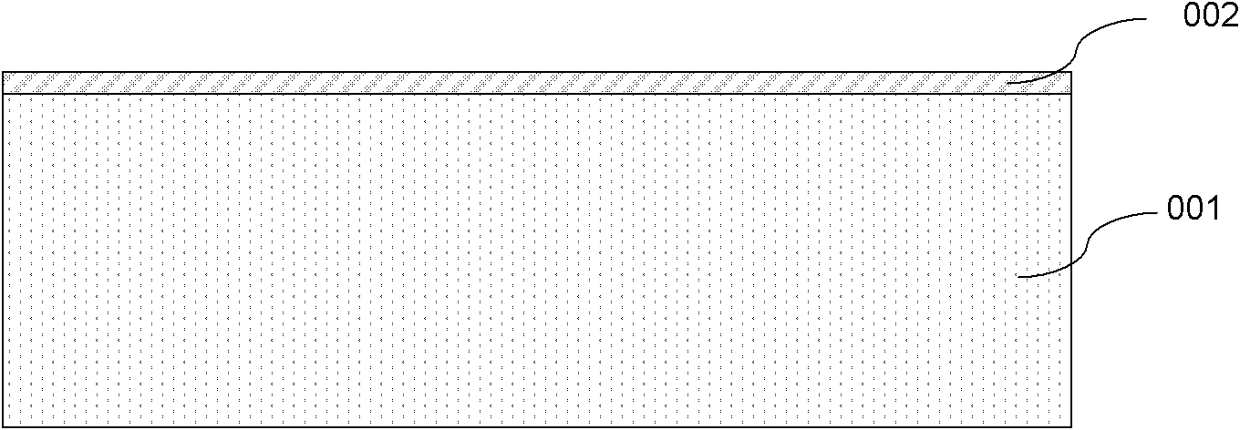
[0039] Executing step S101, providing a oriented monocrystalline silicon substrate on which an oxide layer is formed;

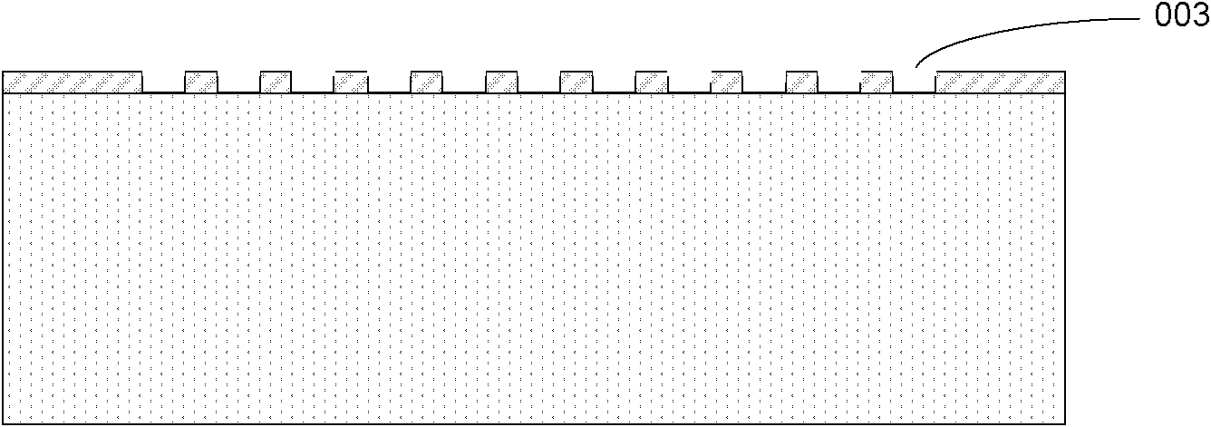
[0040] Execute step S102, using photol...


PUM

PropertyMeasurementUnit
Depthaaaaaaaaaa
Depthaaaaaaaaaa
Thicknessaaaaaaaaaa

Abstract

The invention provides a manufacturing method for a cavity of a full silica-based microfluidic device, comprising the following steps of: providing (111) a crystal-oriented single crystal silicon substrate, on which an oxide layer is formed; patterning the oxide layer, and exposing a plurality of square window patterns; taking the oxide layer as a mask to etch the silicon substrate so as to form an upper-layer deep groove; depositing protection layers on the surface of the oxide layer and on the sidewalls and the bottom of the upper-layer deep groove; removing the protection layer on the surface of the oxide layer and the protection layer on the bottom of the upper-layer deep groove; taking the protection layers on the oxide layer and the protection layer on the sidewalls of the upper-layer deep groove as masks to etch the silicon substrate so as to form a lower-layer deep groove; etching the lower-layer deep groove through a wet etching method, and forming the cavity in the silicon substrate; fully filling holes of the upper-layer deep groove, and sealing off the cavity; and taking the oxide layer as the mask to etch the silicon substrate so as to form four reaction tanks communicated with the cavity. In the manufacturing method provided by the invention, machining is executed based on a single silicon substrate in the cavity forming process, by a mode of firstly forming a bottom cavity in a layering manner and then filling the deep groove, the cavity can be formed without being related to a silica bonding or gluing technology.

Description

technical field [0001] The invention relates to the technical field of biosensor / semiconductor micro-nano manufacturing, in particular, the invention relates to a method for manufacturing a cavity of an all-silicon-based microfluidic device. Background technique [0002] Microfluidic devices are widely used in biomedicine, especially in the precision manufacturing of biomedical devices and the pharmaceutical industry, such as chemical analysis, biological and chemical detection, drug delivery, molecular separation (such as DNA analysis), amplification, sequencing or Nucleic acid synthesis, and environmental monitoring, etc. [Kovacs 1998]. [0003] In the manufacturing process of commonly used biological micro-flow sensors, bulk silicon is usually etched on the surface of the silicon wafer to form a half of the cavity, and then the two parts of the cavity are glued together or formed with silicon / glass and other materials. The silicon wafers of the cavity are bonded to form ...

Claims


Application Information

Patent Timeline
IPC IPC(8): B81C1/00
CPCB81B2203/0315B81C1/00B81C1/00047B01L3/502707B81B2201/058
Inventor 杨海波马清杰吕宇强
Owner ADVANCED SEMICON MFG CO LTD
Why Eureka
Try Eureka