
Method for preparing multi-grade antimonytelluride nano wire harness array by adopting physical vapour deposition

A physical vapor deposition and antimony subtelluride nanotechnology, which is applied in chemical instruments and methods, polycrystalline material growth, ion implantation plating, etc., can solve the problem of general electrical performance of thermal antimony telluride nanowires and difficulty in achieving micro-cooling The linear density requirements of the device and the difficulty of large-scale production have achieved the effects of easy large-scale production, high cooling power density, and low cost.

Active Publication Date: 2012-01-25
HANGZHOU INNOVATION RES INST OF BEIJING UNIV OF AERONAUTICS & ASTRONAUTICS
View PDF2 Cites 7 Cited by
  • Summary
  • Abstract
  • Description
  • Claims
  • Application Information

AI Technical Summary

Problems solved by technology

Due to the many defects in the nanowires prepared by chemical methods, the electrical properties of the thermal antimony telluride nanowires are average, and it is also difficult to produce on a large scale, and it is even more difficult to meet the linear density requirements (5×10 10 / cm 2 )
In addition, the multi-level antimony telluride nanowires and beam arrays prepared by physical methods have not been reported.

Method used


Image

  • Method for preparing multi-grade antimonytelluride nano wire harness array by adopting physical vapour deposition
  • Method for preparing multi-grade antimonytelluride nano wire harness array by adopting physical vapour deposition
  • Method for preparing multi-grade antimonytelluride nano wire harness array by adopting physical vapour deposition

Examples


Embodiment 1

[0037] Example 1: Physical Vapor Deposition of Antimony Telluride Nanowire Arrays on Glass Substrates

[0038] (A) Pressing antimony telluride powder with a mass percent purity of 99.999% into an antimony telluride block under a pressure of 8 MPa; the average particle size of the antimony telluride powder is less than 50 μm;

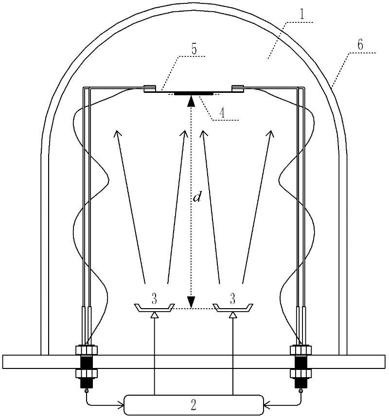
[0039] (B) Put the antimony telluride block into the tungsten boat 3 in the vacuum chamber 1 of the vacuum coating machine, place the glass substrate 4 (or glass plate) on the sample stage 5, and adjust the relationship between the glass substrate 4 and the tungsten boat 3 Distance d=4cm;

[0040](C) Fill the vacuum chamber 1 with nitrogen gas (high-purity nitrogen gas, mass percent purity 99.999%) for 3 minutes and then stop, then fill with nitrogen gas for 3 minutes and then stop, then vacuumize the vacuum chamber 1 to make the vacuum chamber 1 vacuum. up to 2.0×10 -4 Pa;

[0041] (D) Set deposition rate 18nm / min on PID controller 2, deposition ti...

Embodiment 2

[0046] Example 2: Physical Vapor Deposition of Antimony Telluride Nanowire Arrays on CPU Processors

[0047] (A) Pressing antimony telluride powder with a mass percent purity of 99.999% into an antimony telluride block under a pressure of 10 MPa; the average particle size of the antimony telluride powder is less than 50 μm;

[0048] (B) Put the antimony telluride block into the tungsten boat 3 of the vacuum chamber 1 of the vacuum coating machine, place the CPU processor on the sample stage 5, adjust the distance d=6cm between the CPU processor and the tungsten boat 3;

[0049] (C) Fill the vacuum chamber 1 with nitrogen gas (high-purity nitrogen gas, mass percent purity 99.999%) for 5 minutes and then stop, then vacuumize the vacuum chamber 1 so that the vacuum degree in the vacuum chamber 1 reaches 2.0×10 -4 Pa;

[0050] (D) Set deposition rate 15nm / min on PID controller 2, deposition time 5h;

[0051] (E) Turn on the AC power supply and adjust the output current to 170A...

Embodiment 3

[0056] Example 3: Physical Vapor Deposition of Antimony Telluride Nanowire Arrays on Glass Substrates

[0057] (A) Pressing antimony telluride powder with a mass percentage purity of 99.999% into an antimony telluride block under a pressure of 9 MPa; the average particle size of the antimony telluride powder is less than 50 μm;

[0058] (B) Put the antimony telluride block into the tungsten boat 3 of the vacuum chamber 1 of the vacuum coating machine, place the glass substrate 4 on the sample stage 5, and adjust the distance d=8cm between the glass substrate 4 and the tungsten boat 3;

[0059] (C) Fill the vacuum chamber 1 with nitrogen gas (high-purity nitrogen gas, mass percent purity 99.999%) for 3 minutes and then stop, then vacuumize the vacuum chamber 1 so that the vacuum degree in the vacuum chamber 1 reaches 2.5×10 -4 Pa;

[0060] (D) Set deposition rate 10nm / min on PID controller 2, deposition time 7h;

[0061] (E) Turn on the AC power supply, adjust the output cu...


PUM

PropertyMeasurementUnit
particle sizeaaaaaaaaaa
diameteraaaaaaaaaa
diameteraaaaaaaaaa

Abstract

The invention discloses a method for preparing a multi-grade antimonytelluride nano wire harness array by adopting physical vapour deposition. The method comprises the step of depositing multi-grade nano wire harness array antimonytelluride on a glass substrate in vacuum low temperature environment by regulating distance between a glass substrate and a tungsten boat, magnitude of output current of an alternating current power supply and deposition speed of an evaporation source antimonytelluride. Because of low temperature environment, the multi-grade nano wire harness array antimonytelluridecan be deposited on a processor such as a CPU (central processing unit). By applying the method disclosed by the invention, the antimonytelluride nano wire harness array prepared by physical vapour deposition has uniform structure, and uniform distribution of a nano phase is effectively guaranteed.

Description

technical field [0001] The invention relates to a simple physical vapor deposition method to prepare multi-level (multi-size and multi-dimensional point, line, beam) antimony telluride (Sb 2 Te 3 ) nanowire array method. Background technique [0002] The design and processing of low-dimensional nanostructures is an important way to improve the performance of thermoelectric materials. The low-dimensional array technology of thermoelectric materials and the design and realization of special nanostructures are the research frontiers in the field of thermoelectric energy conversion. Among all current thermoelectric materials, Sb 2 Te 3 The semi-conductor materials are currently recognized as the best thermoelectric materials in room temperature and medium temperature regions, and they are already the industry standard for commercial thermoelectric devices. Currently the highest level in the world is Bi as reported by R.Venkatasubramanian 2 Te 3 / Sb 2 Te 3 Superlattice s...

Claims


Application Information

Patent Timeline
Patent Type & Authority Applications(China)
IPC IPC(8): C23C14/24C23C14/06C30B23/02C30B23/06C30B29/46C30B29/62
Inventor 邓元谭明王瑶张志伟梁立新
Owner HANGZHOU INNOVATION RES INST OF BEIJING UNIV OF AERONAUTICS & ASTRONAUTICS
Learn More