GaN (gallium nitride)-based LED (light-emitting diode) with N-type electrodes in dotted distribution and manufacturing method thereof

A light-emitting diode, gallium nitride-based technology, applied in the direction of circuits, electrical components, semiconductor devices, etc., can solve the problems of complex process, lower reliability, increase cost, etc., to simplify the process, improve reliability, and reduce current density Effect

Inactive Publication Date: 2012-01-25
INST OF PHYSICS - CHINESE ACAD OF SCI
View PDF2 Cites 20 Cited by
  • Summary
  • Abstract
  • Description
  • Claims
  • Application Information

AI Technical Summary

Problems solved by technology

However, the process of preparing bridge electrode connections on the surface of GaN chips is complex, and the insulating dielectric layer under the bridge connections is also limited, which reduces reliability and increases costs.

Method used


Image

  • GaN (gallium nitride)-based LED (light-emitting diode) with N-type electrodes in dotted distribution and manufacturing method thereof
  • GaN (gallium nitride)-based LED (light-emitting diode) with N-type electrodes in dotted distribution and manufacturing method thereof
  • GaN (gallium nitride)-based LED (light-emitting diode) with N-type electrodes in dotted distribution and manufacturing method thereof

Examples


Embodiment Construction

[0023] In order to make the object, technical solution and advantages of the present invention clearer, the present invention will be described in further detail below in conjunction with specific embodiments and with reference to the accompanying drawings.

[0024] The reference signs involved therein are explained as follows:

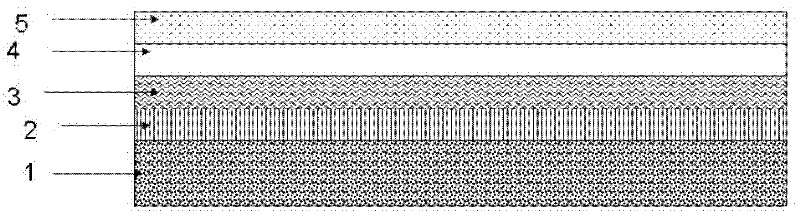
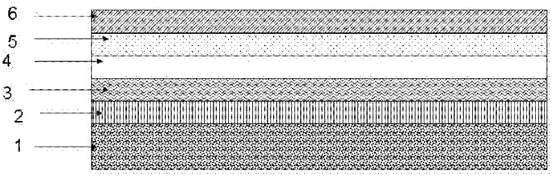
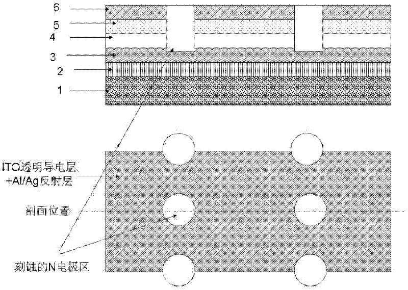
[0025] 1. Sapphire substrate

[0026] 2. Buffer layer

[0027] 3. N-GaN layer

[0028] 4. Multiple quantum well layers

[0029] 5. P-GaN layer

[0030] 6. ITO transparent conductive layer + Al / Ag reflective layer

[0031] The preparation method of the GaN-based flip-chip light-emitting diode with dotted N-electrode structure proposed by the present invention specifically includes the following steps:

[0032] Such as figure 1 As shown, on a sapphire substrate 1, a buffer layer 2, an N-GaN layer 3, a multi-quantum well layer 4, a P-GaN layer 5, etc. are sequentially grown to form a GaN-based LED epitaxial wafer.

[0033] Such as figure 2 As sh...


PUM

PropertyMeasurementUnit
diameteraaaaaaaaaa
diameteraaaaaaaaaa

Abstract

The invention relates to a GaN (gallium nitride)-based flip-chip LED (light-emitting diode) with N-type electrodes in dotted distribution and a manufacturing method thereof. The LED comprises a GaN-based chip and a flip-chip-bonding substrate which is bonded with the GaN-based chip by a flip chip bonding method. In the manufacturing method, a metallorganic chemical vapor deposition growth technology is adopted to grow a multilayer material structure of the GaN-based LED on a heterogeneous material or sapphire substrate, and the main manufacturing processes of the device such as photoetching, deposition, etching, evaporation, sputtering and peeling are carried out to realize P-type reflecting layer electrodes and N-type electrodes of the flip-chip-bonding chip. In the method, multiple N-type electrodes in dotted distribution is adopted, and the flip-chip-bonding substrate is utilized to be connected with the N-type electrodes, thus the P-type region area is increased and the process complexity is lowered at the same time, the reliability is improved, and the luminous efficiency of the flip-chip-bonding LED chip is improved greatly.

Description

technical field [0001] The invention relates to the technical field of semiconductor lighting, in particular to a gallium nitride-based flip-chip light-emitting diode with a point-like distributed N electrode structure and a preparation method thereof. Background technique [0002] In the field of semiconductor lighting, the light loss on the non-light-exiting end face has always been one of the problems that it is difficult to increase the luminous efficiency of flip-chip LED chips. Gallium nitride (GaN)-based compound semiconductor materials have a wide band gap and a direct band gap. , can be used to make green, blue and ultraviolet LEDs. On the basis of ordinary LEDs, by increasing the size of the die, the so-called large die LED, the luminous power can be improved. At the same time, in order to further improve the luminous power and facilitate the heat dissipation of the device, Flip-chip welding technology is usually used to flip-chip-bond GaN-based large die LEDs on t...

Claims


Application Information

Patent Timeline
Patent Type & Authority Applications(China)
IPC IPC(8): H01L33/38
Inventor 贾海强陈弘王文新李卫江洋王禄
Owner INST OF PHYSICS - CHINESE ACAD OF SCI
Why Eureka
Try Eureka