All-band reverse optical detector constructed on basis of organic small molecular material

An optical detector, full-band technology, applied in photovoltaic power generation, electric solid state devices, semiconductor devices and other directions, can solve the problems of high cost, high operating voltage, complex material manufacturing process, etc., to achieve low cost, easy device structure, spectral Responsive effect

Inactive Publication Date: 2012-03-21
CHANGCHUN INST OF OPTICS FINE MECHANICS & PHYSICS CHINESE ACAD OF SCI
View PDF3 Cites 12 Cited by
  • Summary
  • Abstract
  • Description
  • Claims
  • Application Information

AI Technical Summary

Problems solved by technology

In addition, although inorganic materials can be used to make full-band photodetectors, the operating voltage of inorganic f

Method used


Image

  • All-band reverse optical detector constructed on basis of organic small molecular material
  • All-band reverse optical detector constructed on basis of organic small molecular material

Examples


preparation example Construction

[0027] The preparation method of the present invention: deposit the first electron donor layer on the hole collecting electrode layer; deposit the first electron acceptor layer on the electron donor layer; The bulk layer; then the exciton blocking layer is prepared by dual-source co-deposition method; finally, the first electron collecting electrode layer and the second electron collecting electrode layer are deposited; the above-mentioned layers all adopt vacuum thermal deposition process.

[0028] The substrate is made of glass, and the hole-collecting electrode layer (transparent conductive film) is made of indium tin oxide ITO transparent conductive film; the first electron donor layer is made of m-MTDATA or 2-TNATA, or a mixture thereof, and the mixing mass ratio is 9:1, the thickness is selected from 1 to 20nm; the first electron acceptor layer (and the second electron donor layer) is selected from CuPc or TiOPC, and the thickness is selected from 2 to 40nm; the second el...

Embodiment 1

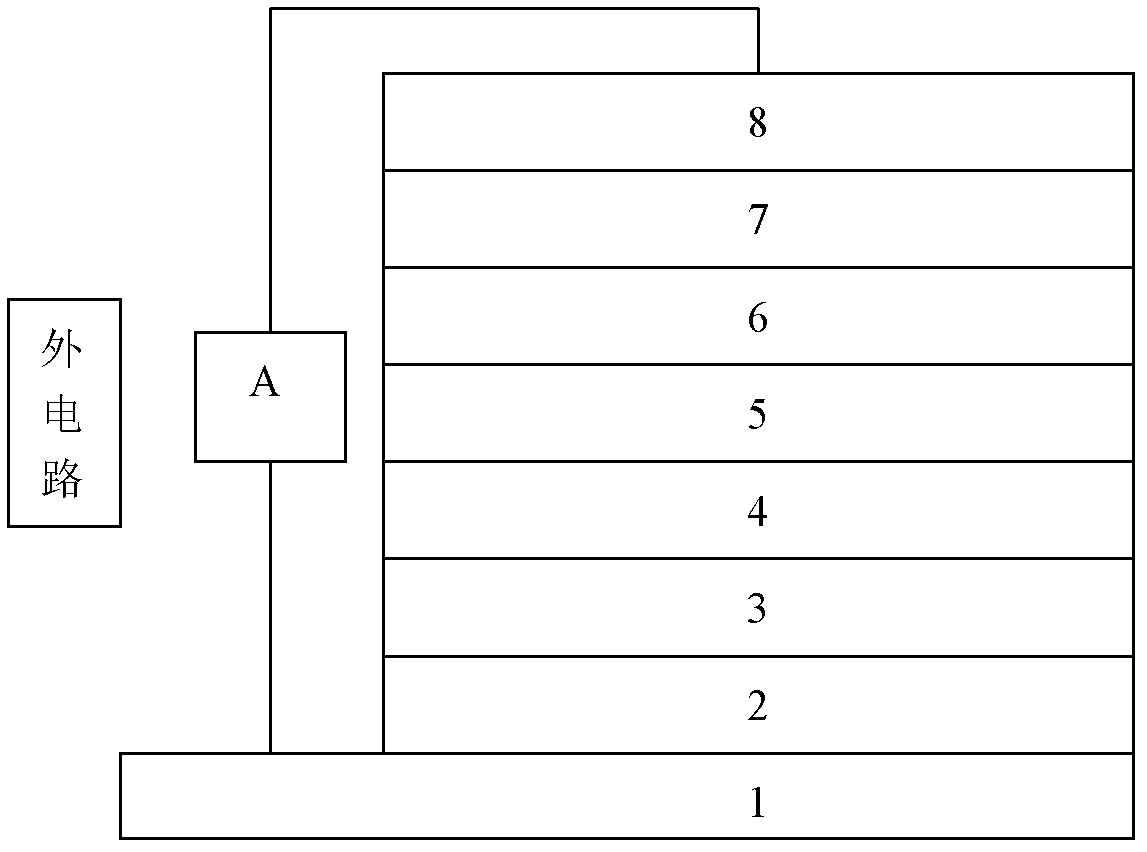
[0031] select figure 1 The device structure shown: In this embodiment, firstly, the hole-collecting electrode layer 2 selects the indium tin oxide ITO film on the glass substrate 1 as the transparent conductive film. After cleaning the transparent conductive film on the substrate 1, at first in high vacuum (3~2×10 -4 Pa), on the transparent conductive film 2, deposit a layer of thickness and be the first electron donor layer 3 of 10nm, the material of the first electron donor layer 3 adopts m-MTDATA; Then deposit 30nm on the first electron donor layer 3 The first electron acceptor layer 4, the material of the first electron acceptor layer 4 adopts TiOPc; The second electron acceptor layer 5 of 10nm is deposited on the first electron acceptor layer 4, the material of the second electron acceptor layer 5 Use F 16 A mixture layer of CuPc and PTCDI-C8, the mixing mass ratio of the two is 1:1; a 10nm exciton blocking layer 6 is deposited on the second electron acceptor layer 5, a...

Embodiment 2

[0033] select figure 1 The device structure shown: the hole collection electrode layer 2 selects the indium tin oxide ITO film on the glass substrate 1 as the transparent conductive film; the material of the first electron donor layer 3 is 2-TNATA, and the thickness is 15nm; The first electron acceptor layer 4 of 30nm is deposited on the electron donor layer 3, the material of the first electron acceptor layer 4 adopts TiOPc; Then the second electron acceptor layer 5 of 5nm is deposited on the first electron acceptor layer 4 , the material of the second electron acceptor layer 5 adopts F 16 A mixture layer of CuPc and PTCDI-C8, the mixing mass ratio of the two is 1:1; a 5nm exciton blocking layer 6 is deposited on the second electron acceptor layer 5, and the material of the exciton blocking layer 6 adopts a mass fraction of 3% Ce 2 CO 3 Doped Bphen; on the exciton blocking layer 6, deposit the first electron collecting electrode layer 7 of 10nm, the material of the first el...


PUM

PropertyMeasurementUnit
Thicknessaaaaaaaaaa
Thicknessaaaaaaaaaa
Thicknessaaaaaaaaaa

Abstract

The invention discloses an all-band reverse optical detector constructed on the basis of an organic small molecular material, and belongs to the field of organic optical detectors made of organic small molecular materials. The detector has a lamellar structure, and sequentially comprises a glass substrate coated with a conductive film, a hole collecting electrode layer indium tin oxide conductive film, a first electron donor layer, a first electron acceptor layer and the like, wherein the thickness of the first electron donor layer is 1 to 20 nanometers; the first electron acceptor layer serves as a second electron donor layer, and the thickness of the first electron acceptor layer is 2 to 40 nanometers; the thickness of a second electron acceptor layer is 5 to 20 nanometers; the thickness of an exciton barrier layer is 5 to 15 nanometers; the thickness of a first electron collecting electrode layer is 5 to 10 nanometers; and the thickness of a second electron collecting electrode layer is 10 to 30 nanometers. The all-band reverse optical detector has a simple making process and low cost, and market sold organic materials can be adopted; and because combination of multiple organic layers of a film is adopted, the design of the detector is more flexible.

Description

technical field [0001] The invention belongs to the field of organic optical detectors composed of organic small molecule materials, in particular to full-band optical detector devices sensitive to sun-blind ultraviolet light, visible light and near-infrared light. Background technique [0002] The requirement of the organic material optical detector in the prior art is to use the photovoltaic effect to convert the optical signal into a corresponding electrical signal when a negative voltage is applied to it, and to detect the power of the incident light by measuring the electrical signal, and the work of the detector The performance is judged by the external quantum efficiency and response time of photoelectric conversion. At present, more researches in this field are optical detectors sensitive to ultraviolet light and near-infrared light. Although there have been relevant reports in the prior art on the full-band optical detectors from sun-blind ultraviolet light, visibl...

Claims


Application Information

Patent Timeline
IPC IPC(8): H01L51/42H01L51/46
CPCY02E10/549Y02P70/50
Inventor 苏子生初蓓李文连吴双红
Owner CHANGCHUN INST OF OPTICS FINE MECHANICS & PHYSICS CHINESE ACAD OF SCI
Why Eureka
Try Eureka