Method for manufacturing chip inductance element from low-temperature cofired ferrite raw material belt

A ferrite raw material, low temperature co-firing technology, applied in electrical components, inductors, fixed inductors, etc., can solve the problem of high Curie temperature, achieve high Curie temperature, uniform distribution, and prevent device failure.

Active Publication Date: 2012-04-11
JIANGSU HUAXING ELECTRONICS CO LTD
View PDF5 Cites 16 Cited by
  • Summary
  • Abstract
  • Description
  • Claims
  • Application Information

AI Technical Summary

Problems solved by technology

For ferrite materials, high initial magnetic permeability and high Curie temperature are required, but these two are contradictory. The existing ferrite raw materials used in the production of chip inductors on the market are difficult to maintain High initial permeability and high Curie temperature

Method used


Image

  • Method for manufacturing chip inductance element from low-temperature cofired ferrite raw material belt
  • Method for manufacturing chip inductance element from low-temperature cofired ferrite raw material belt
  • Method for manufacturing chip inductance element from low-temperature cofired ferrite raw material belt

Examples


Embodiment 1

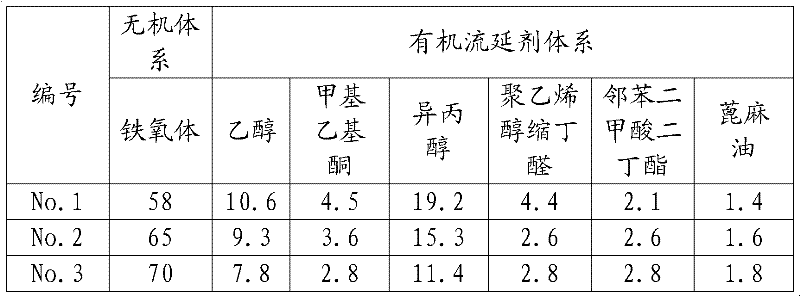
[0031] Table 1 shows the content of each component of the specific example 1 of the present invention. Weigh the calcined ferrite powder according to the formula in Table 1, add solvent and dispersant and ball mill for 3-6 hours, add binder and plasticizer and ball mill for 3-6 hours, vacuum defoaming, tape casting, and drying to obtain The low-temperature co-fired ferrite raw tape of the present invention.

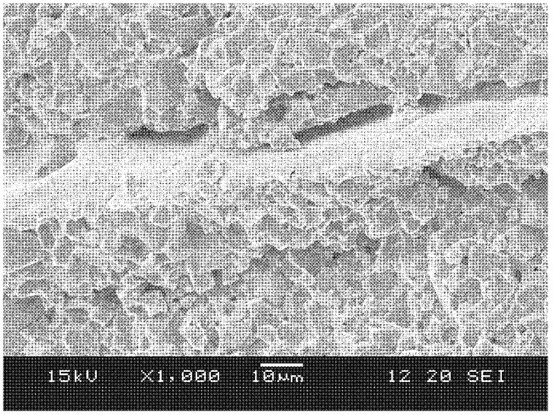
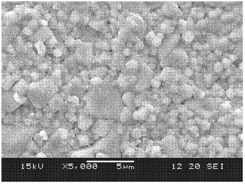
[0032] In the present invention, the prepared raw material tape is engraved to make a standard test ring, the temperature is raised at 2°C / min to 450°C for 3 hours to remove glue, and then the temperature is raised from 450°C to 900°C for 3 hours at 2.5°C / min for sintering. During the cooling process, the temperature was controlled to drop to 250°C for 10 hours, and then cooled naturally with the furnace, and the performance of the sintered body was tested (see Table 2).

[0033] Table 1 The content of each component of low temperature co-fired ferrite raw tape (wt%)

...

Embodiment 2

[0038] Table 4 shows the content of each component of the specific example 2 of the present invention. Weigh the calcined ferrite powder according to the formula in Table 4, add solvent and dispersant and ball mill for 3-6 hours, add binder and plasticizer and ball mill for 3-6 hours, vacuum defoaming, tape casting, and drying to obtain The low-temperature co-fired ferrite raw tape of the present invention.

[0039] In the present invention, ring-cutting is performed on the prepared raw material tape, the temperature is raised to 450°C at 2°C / min and kept for 3 hours to remove glue, and then the temperature is raised from 450°C to 900°C for 3 hours at 2.5°C / min for sintering. During the cooling process, the temperature was controlled to drop to 250°C for 10 hours, and then cooled naturally with the furnace, and the performance of the sintered body was tested (see Table 5).

[0040] Table 4 The content of each component of low temperature co-fired ferrite raw tape (wt%)

[00...


PUM

PropertyMeasurementUnit
electrical resistivityaaaaaaaaaa

Abstract

The invention relates to a method for manufacturing a chip inductance element from a low-temperature cofired ferrite raw material belt. The method comprises the following steps of: 1, preparing the low-temperature cofired ferrite raw material belt; and 2, preparing the chip inductance element: positioning and drilling on the ferrite raw material belt according to the structure of a chip inductor; filling a through hole with a silver paste by adopting a screen printing method; printing a silver paste conductor pattern on the raw material belt, and printing a layer of low-temperature glass protective coating on the surface of the silver paste pattern; placing the printed raw material belt into a closely-laminated die in turn according to pre-designed layer number and order, and isopressing to form a complete multilayer base plate blank; dividing the multilayer base plate blank into small specific blocks, placing the small specific blocks into a furnace, raising the temperature to 450 DEG C, keeping the temperature for 3 hours, discharging rubber, raising the temperature from 450 DEG C to 900 DEG C, maintaining the temperature for 3 hours, and sintering; controlling the temperature for 10 hours during cooling until the temperature is 250 DEG C, and then naturally cooling along with the furnace; and manufacturing an electrode by brushing silver and capping the end of the sintered electronic element to obtain the chip inductance element.

Description

technical field [0001] The invention relates to the technical field of making chip inductance elements from magnetic materials, in particular to a method for making chip inductance elements from low-temperature co-fired ferrite raw materials. Background technique [0002] Inductance has no resistance to DC current, but has resistance to AC current. When a direct current is passed through the inductor, only fixed magnetic lines of force appear around it, which do not change with time; but when an alternating current is passed through the coil, magnetic lines of force that change with time will appear around it. This allows the chip inductance element to be applied to high-frequency nanohenry inductors in mobile communication terminals and the like. Chip multilayer inductors are small in size, high in integration, short and thin, which is conducive to the miniaturization of the circuit; the magnetic circuit is closed, it will not interfere with the surrounding components, and...

Claims


Application Information

Patent Timeline
Patent Type & Authority Applications(China)
IPC IPC(8): H01F41/00H01F37/00C04B35/26C04B35/622
Inventor 朱海奎徐志明周洪庆赵建新张一源余捷
Owner JIANGSU HUAXING ELECTRONICS CO LTD
Why Eureka
Try Eureka