Silver alloy target for forming reflection electrode film for organic el element, and method for manufacturing the silver alloy target
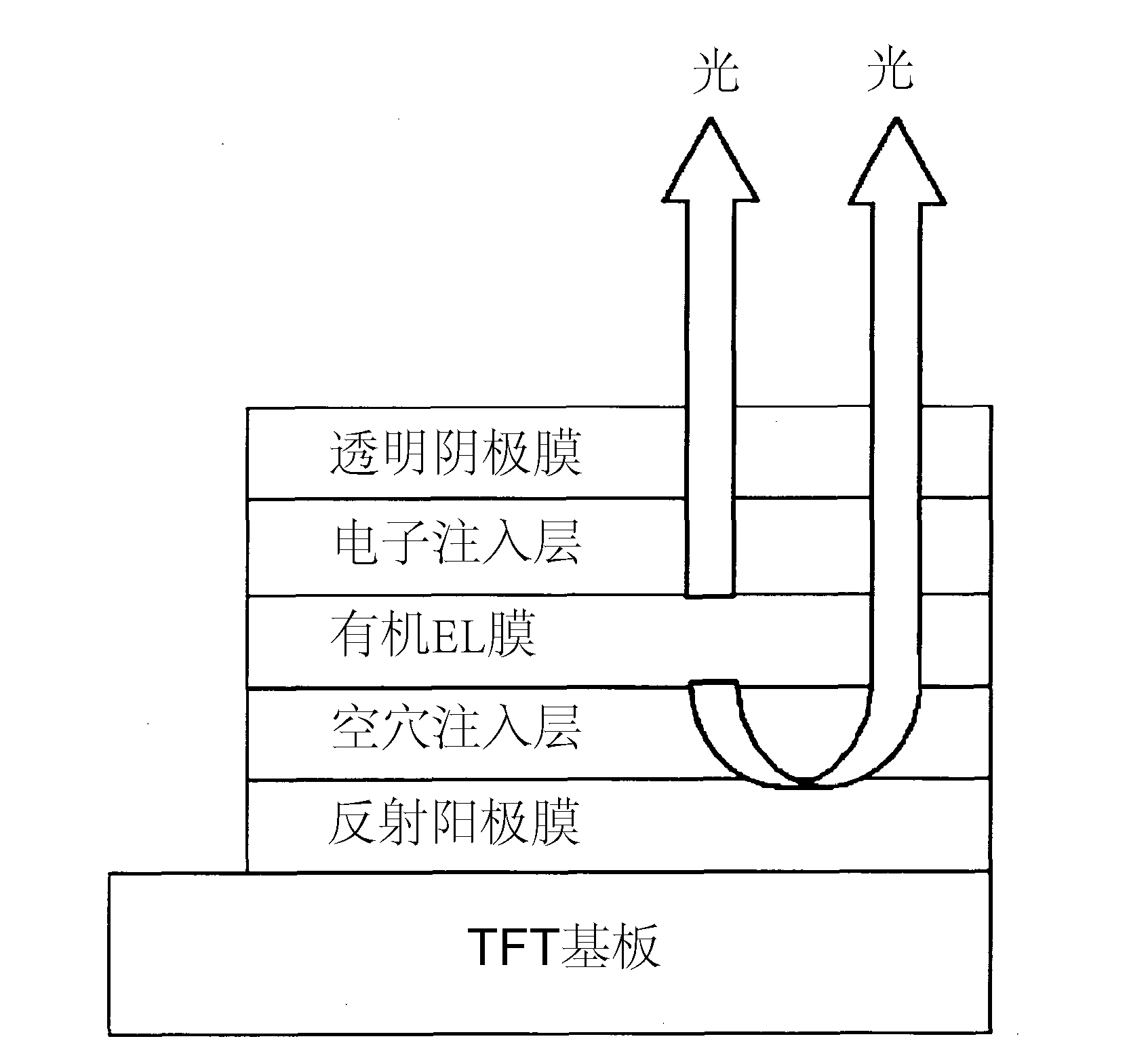
A technology of a reflective electrode film and a manufacturing method, which is applied in the manufacture of semiconductor/solid-state devices, electrical components, circuits, etc., can solve the problems of short circuit and the reduction of the qualification rate of organic EL components, and achieve high reflectivity, suppression of splashes, and suppression of abnormality. The effect of discharge
- Summary
- Abstract
- Description
- Claims
- Application Information
AI Technical Summary
Problems solved by technology
Method used
Image
Examples
Embodiment 1)
[0041] (Example 1) [Manufacture of silver alloy target]
[0042] As raw materials, Ag with a purity of 99.99% by mass or higher and In with a purity of 99.9% by mass or higher were prepared, and Ag and In were filled in a high-frequency vacuum melting furnace at a mass ratio shown in Table 1 as raw materials. The total mass when melted is about 300kg.
[0043] After evacuating the vacuum chamber, it was replaced with Ar gas, and after Ag was melted, In was added, and the molten alloy was cast in a graphite mold. The shrinkage cavity portion in the upper part of the ingot produced by casting was cut off, and an ingot (φ290×370 mm) of about 260 kg was obtained as a complete part.
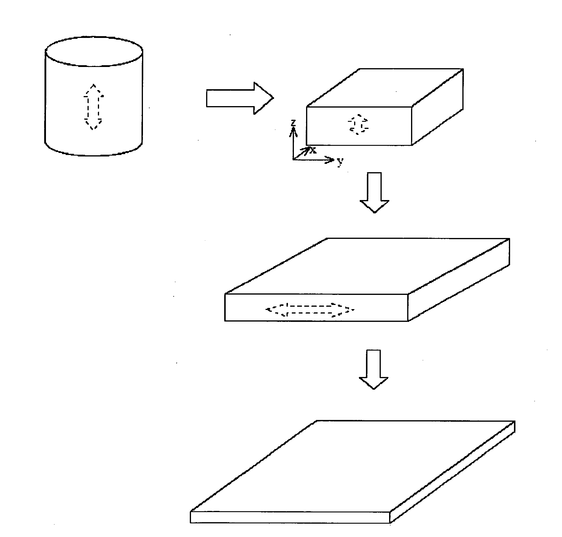
[0044] After the obtained ingot was heated at 750-850°C for 1 hour, the forging direction was repeatedly turned 90° each time, relative to the casting direction z, any direction x of 90° relative to z, and 90° relative to z and x ° direction y in all directions, for forging. Make the single forging...
Embodiment 2~4、 comparative example 1~8)
[0061] Except for the component composition and manufacturing conditions described in Table 1, targets were produced in the same manner as in Example 1, and after obtaining silver alloy targets in Examples 2-4 and Comparative Examples 1-8, various evaluations were performed in the same manner as in Example 1. The results are shown in Table 1 and Table 2.
[0062] (existing example 1, 2)
[0063] The composition of In described in Table 1 was melted in the same manner as in Example 1, cast into a square graphite mold to produce an ingot of about 400×400×150 (mm), and the ingot was further heated at 600°C Hot rolling was performed after 1 hour, and the silver alloy target of Conventional Example 1 was produced. In addition, the cast ingot was hot-rolled in the same manner as in Conventional Example 1, and then heat-treated at 600° C. for 2 hours to produce a silver alloy target in Conventional Example 2. Various evaluations were performed in the same manner as in Example 1 usi...
reference example 1)
[0065] The mixing ratio of In recorded in Table 1 was melted with a charge weight of 7 kg, and the alloy melt was cast in a graphite mold to produce an ingot of φ80×110 (mm), and the obtained ingot was used for comparison with Comparative Example 3 The same number of times of upsetting, cold rolling reduction, heat treatment, to obtain a 220 × 220 × 11 (mm) plate. Various evaluations were performed in the same manner as in Examples and Comparative Examples. The results are shown in Table 1 and Table 2. However, since the target of Reference Example 1 was smaller in size than the targets produced in Examples and Comparative Examples, warpage after machining was not evaluated.
[0066]
[0067]
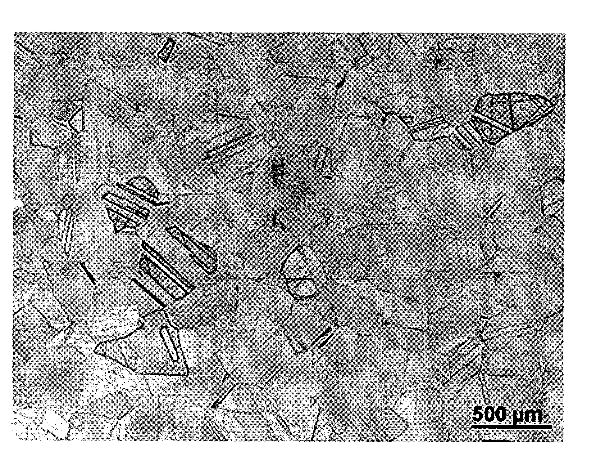
[0068]It can be seen from Table 1 that for Examples 1-4, the average grain size of the silver-indium alloy crystal grains is 160-360 μm, and the grain size deviation is good at 12-18%. On the other hand, in Comparative Example 3 in which the number of times of upsetting was 5, t...
PUM
| Property | Measurement | Unit |
|---|---|---|
| particle diameter | aaaaa | aaaaa |
| particle diameter | aaaaa | aaaaa |
| roughness | aaaaa | aaaaa |
Abstract
Description
Claims
Application Information


