Method for removing polished section crystal round edge used for IGBT (insulated gate bipolar transistor) in a row grinding manner

A polishing wafer and oxide film technology, applied in the field of back treatment, can solve the problems of reducing the effective area of ​​epitaxy, operator injury, high cost and high cost, and achieve the effect of being conducive to mass production, improving production efficiency and high production efficiency

Active Publication Date: 2012-05-02
ZHONGHUAN ADVANCED SEMICON MATERIALS CO LTD +1
View PDF3 Cites 15 Cited by
  • Summary
  • Abstract
  • Description
  • Claims
  • Application Information

AI Technical Summary

Problems solved by technology

Edge oxide film removal is an important process in the processing of silicon wafer polishing, which plays a vital role in the yield of polished wafers, subsequent epitaxy and IGBT devices: chamfers, silicon wafers caused by the back-sealing process Front SiO 2 Residues, even SiO on the back edge of the wafer 2 Residues may become nucleation centers during epitaxial growth, forming polycrystalline and amorphous (amorphous silicon) at the edge; thus affecting the quality of epitaxial growth and reducing the effective area of ​​epitaxial growth
The lattice defects at the edge of the epitaxy can cause the edge yield of the device to be low
[0003] Unfortunately, at present, domestic wafer manufacturers have their own limitations in the edge oxide film removal treatment technology: usually include the following methods: Method 1 is: use HF gas to remove the oxide film on the edge of the silicon wafer in the reaction chamber (abbreviated in the text) Reaction chamber edge removal technology), the disadvantage of this technology is that HF ​​gas is volatile, and a large amount of HF will be consumed for one corrosion, which is not conducive to cost control, and may also cause harm to operators; in addition, the range of HF removal cannot be precisely controlled, which may cause Back-sealed SiO in the center of the backside of the silicon wafer 2 remove the membrane
[0004] Method 2: Align the rack with the silicon wafers on the runner, so that the silicon wafers are in contact with the runner (referred to as the roller-type edge removal technology in the text); use the runner to drive the ra

Method used


Image

  • Method for removing polished section crystal round edge used for IGBT (insulated gate bipolar transistor) in a row grinding manner
  • Method for removing polished section crystal round edge used for IGBT (insulated gate bipolar transistor) in a row grinding manner

Examples


Embodiment 1

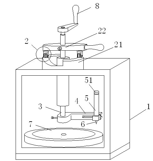
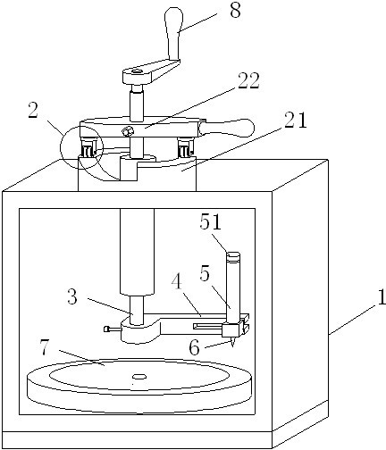
[0042] The traditional method of pasting the special blue film by hand in the present invention is changed to use a scratch-type semi-automatic edge removal machine to prepare circular plastic blue films of different specifications, thereby completing the removal of the oxide film on the back of the wafer. Concrete preparation process is as follows:

[0043] 1) Prepare a 6-inch (diameter 150mm) single-crystal silicon wafer with a thickness of 642 μm, As dopant, crystal orientation, and a resistivity of 0.002-0.004 after back damage and back sealing; prepare a plastic blue film As an auxiliary material, the material is PVC, the thickness is 380μm, the width is 160mm, and the length of a roll is 10m;

[0044] 2) Take it out of the blue film, with the back cover facing down and the front facing up, and stick them on the roll plastic blue film in turn,

[0045] 3) After the heat shrinking machine is preheated, pass the rolled plastic blue film adhered to the silicon wafer th...


PUM


Abstract

The invention relates to a method for removing a polished section crystal round edge used for an IGBT (insulated gate bipolar transistor) in a row grinding manner. The method is characterized in that a special cutting edge machine is applied to a polished section crystal round edge oxide film treatment process, and firstly, a package plastic blue film is adhered on a silicon die back surface through a pyrocondensation machine; the special cutting edge machine marks different sizes of roundness incisions on the plastic blue film adhered on the silicon die back surface according to different specification of a silicon slice, the annular roundness plastic blue film required to be corroded is torn up along the incisions, thereby protecting the part of which a back sealed Si02 film is not required to remove; the row ground type cutting edge technology can be used for preparing a raw material substrate of an epitaxial wafer used for electric power electron devices such as IGBT and the like;and the method provided by the invention has the advantages of simple operation, low cost, high production efficiency, strong practicability, and is technology which is suitable for removing the backSi02 film in large-scale industry production.

Description

technical field [0001] The invention relates to a back treatment technology of a semiconductor wafer silicon polishing sheet, in particular to a method for removing an oxide film on the edge of a polishing sheet used for IGBTs by means of scratching. Background technique [0002] With the rapid development of China's economy, various domestic infrastructure and energy construction are in a period of rapid development. A number of national key projects that have a huge stimulating effect on the national economy, represented by the State Grid Project, high-speed rail transit, electric vehicles and hybrid vehicles, and green energy-saving industries, all have strong demand for new power electronic devices. With the rapid growth of new power electronic devices represented by IGBT, the development of polished silicon wafers, the raw material substrate for IBGT epitaxial wafers, provides a broad market space and rare opportunities. The processing of polished silicon wafe...

Claims


Application Information

Patent Timeline
IPC IPC(8): H01L21/304
Inventor 刘振福张宇王瑶李翔
Owner ZHONGHUAN ADVANCED SEMICON MATERIALS CO LTD
Why Eureka
Try Eureka