

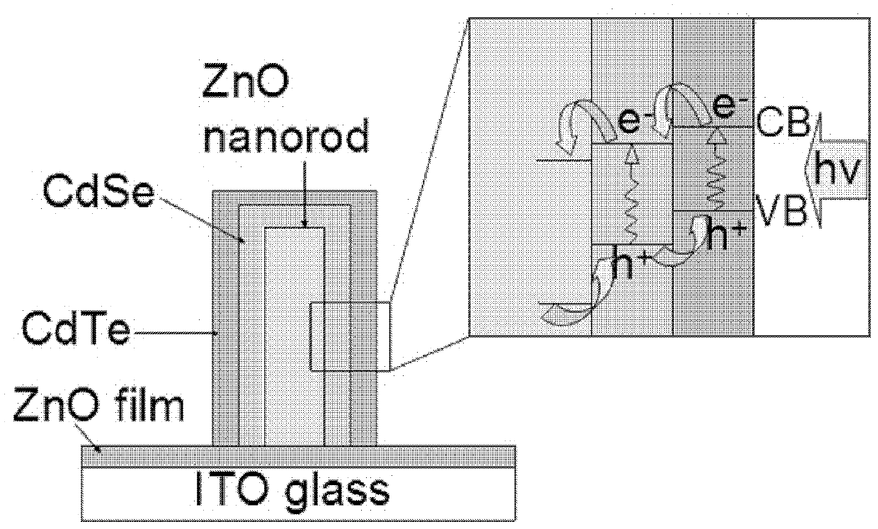
ZnO/CdSe/CdTe nanorod array photoelectrode and preparation method thereof
A nanorod array and photoelectrode technology, which is applied in the manufacture of circuits, electrical components, and final products, can solve the problems of limited range of absorption spectrum, poor chemical and electrical stability, difficult control and repetition, etc., to reduce electronic recombination loss , high interface quality, improved light absorption efficiency and photoelectrochemical properties
- Summary
- Abstract
- Description
- Claims
- Application Information
AI Technical Summary
Problems solved by technology
Method used
Image

Examples
Embodiment 1
[0139] Embodiment 1: Preparation of ZnO / CdSe / CdTe nanorod array photoelectrode
[0140] The preparation steps are as follows:
[0141] A. Surface pretreatment of ITO conductive glass
[0142] The surface of ITO conductive glass is ultrasonically cleaned with deionized water, acetone, alcohol and deionized water for 15 minutes, then dried with a hair dryer, and immediately transferred to the radio frequency magnetron sputtering coating machine produced by Chengdu Qixing Vacuum Coating Technology Co., Ltd. , at a vacuum of 10 ~3 Protected under the condition of Pa;
[0143] B, preparation of ZnO buffer film layer
[0144] Put the clean ITO conductive glass obtained in step A) in the radio frequency magnetron sputtering coater, and use the ITO glass as the anode substrate to sputter the cathode ZnO target for 20 minutes under the conditions of heating temperature 200°C and vacuum degree 0.1Pa, and grow One layer of ZnO buffer film layer;
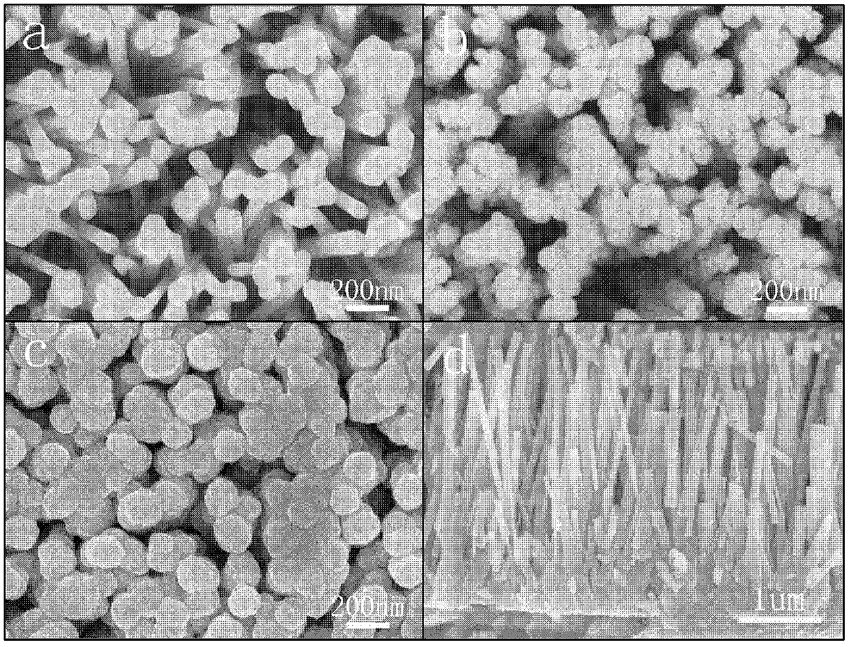
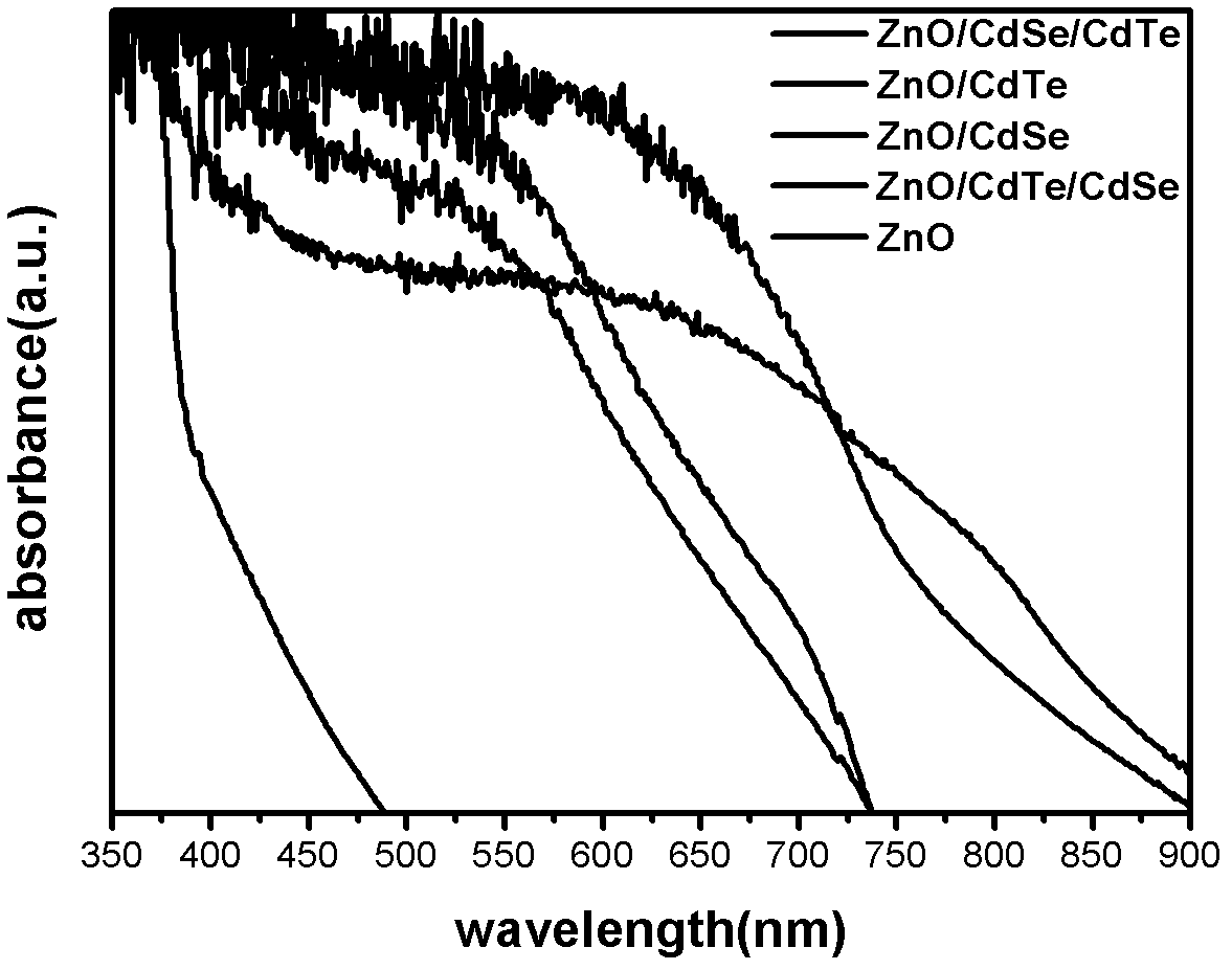
[0145] C, preparation of ZnO nanoro...
Embodiment 2
[0161] Embodiment 2: Preparation of ZnO / CdSe / CdTe nanorod array photoelectrode
[0162] The preparation steps are as follows:
[0163] A. Surface pretreatment of ITO conductive glass
[0164] The surface of the ITO conductive glass is ultrasonically cleaned with deionized water, acetone, alcohol and deionized water for 25 minutes, then dried with a hair dryer, and immediately transferred to the RF magnetron sputtering coating machine produced by Chengdu Qixing Vacuum Coating Technology Co., Ltd. , at a vacuum of 10 ~5 Protected under the condition of Pa;
[0165] B, preparation of ZnO buffer film layer
[0166] The clean ITO conductive glass obtained in step A) is placed in the radio frequency magnetron sputtering coating machine, the ITO glass is used as the anode substrate, and the cathode ZnO target is sputtered for 25 minutes at a heating temperature of 300° C. and a vacuum degree of 10 Pa to grow a Layer ZnO buffer film layer;
[0167] C, preparation of ZnO nanorod a...
Embodiment 3
[0182] Embodiment 3: Preparation of ZnO / CdSe / CdTe nanorod array photoelectrode
[0183] The preparation steps are as follows:
[0184] A. Surface pretreatment of ITO conductive glass
[0185] The surface of ITO conductive glass is ultrasonically cleaned with deionized water, acetone, alcohol and deionized water for 20 minutes, then dried with a hair dryer, and immediately transferred to the radio frequency magnetron sputtering coating machine produced by Chengdu Qixing Vacuum Coating Technology Co., Ltd. , at a vacuum of 10 ~4 Protected under the condition of Pa;
[0186] B, preparation of ZnO buffer film layer
[0187] Place the clean ITO conductive glass obtained in step A) in the radio frequency magnetron sputtering coater, and sputter for 30 minutes under the conditions of a heating temperature of 250° C. and a vacuum of 5 Pa to grow a ZnO buffer film layer;
[0188] C, preparation of ZnO nanorod array layer
[0189] In the same way as in Example 1
[0190] Weigh 0.0...
PUM
| Property | Measurement | Unit |
|---|---|---|
| Thickness | aaaaa | aaaaa |
| Thickness | aaaaa | aaaaa |
| Diameter | aaaaa | aaaaa |
Abstract
Description
Claims
Application Information