Surface plasmon laser of semiconductor nanowire-metal film structure

A surface plasmon and metal thin film technology, applied in the field of nano optics, can solve problems such as the difficulty in reaching the excitation laser threshold, the inability to realize the resonance effect of long-wavelength visible light nano-laser, and the difficulty of sub-wavelength nano-laser.

Active Publication Date: 2012-05-02
SOUTHEAST UNIV
View PDF5 Cites 15 Cited by
  • Summary
  • Abstract
  • Description
  • Claims
  • Application Information

AI Technical Summary

Problems solved by technology

In the high-frequency visible light band, metals have high ohmic losses, and it is difficult to achieve the threshold conditions required for laser excitation. Therefore, it is difficult to realize high-quality sub-wavelength nanolasers by using semiconductor nanowires as gain media. The nano-laser resonance effect in the long-wave visible and infrared bands cannot meet the actual needs of the future nano-optical communication field.

Method used


Image

  • Surface plasmon laser of semiconductor nanowire-metal film structure
  • Surface plasmon laser of semiconductor nanowire-metal film structure
  • Surface plasmon laser of semiconductor nanowire-metal film structure

Examples


Embodiment 1

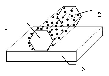
[0037] The surface plasmon laser of the semiconductor nanowire-metal thin film structure of the present embodiment mainly includes figure 1 , figure 2 Two structures, structure 1 includes solid semiconductor nanowires 1, quantum dots 2 and metal film 3, solid semiconductor nanowires 1 are closely attached to the surface of metal film 3, there is no gap between them, quantum dots 2 are distributed on solid semiconductor nanowires 1 surface.

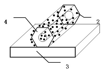
[0038] figure 2 The structure includes hollow semiconductor nanowires 4, quantum dots 2 and metal thin film 3, the hollow semiconductor nanowires 4 are closely attached to the surface of the metal thin film 3, there is no gap therebetween, and the quantum dots 2 are distributed on the outer surface and inner wall of the hollow semiconductor nanowires 4 superior. figure 2 The structure of the semiconductor nanowire is hollowed out by using technologies such as electron beam penetration to form a hollow nanowire 4, and quantum dots ar...

Embodiment 2

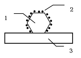
[0043] This example has Figure 8 , Figure 9 two structures, Figure 8 The structure includes a solid semiconductor nanowire 1, quantum dots 2 and a metal film 3, the quantum dots 2 are distributed on the surface of the solid semiconductor nanowire 1, there is a gap between the solid semiconductor nanowire 1 and the surface of the metal film 3, and at least A layer of quantum dots 2 .

[0044] Figure 9 The structure includes a hollow semiconductor nanowire 4, quantum dots 2 and a metal film 3, the quantum dots 2 are distributed on the outer surface and the inner wall of the hollow semiconductor nanowire 4, there is a gap between the hollow semiconductor nanowire 4 and the surface of the metal film 3, the gap There is at least one layer of quantum dots 2 distributed in it. Figure 9 The structure of the semiconductor nanowire is hollowed out by using technologies such as electron beam penetration to form a hollow nanowire 4, and quantum dots are distributed on the surface...


PUM


Abstract

The invention relates to a surface plasmon laser of a semiconductor nanowire-metal film structure, which mainly consists of a solid semiconductor nanowire, a hollow semiconductor nanowire, quantum dots and a metal film. The surface plasmon laser is of the semiconductor nanowire-metal film structure densely provided with the quantum dots, the semiconductor nanowire emits high-frequency laser underexternal excitation, the high-frequency laser is absorbed by the quantum dots on the surface of the nanowire, and low-frequency light is radiated, thus the wavelength of the laser is modulated, and asurface plamon mode is excited on the surface of the metal film. A plurality of light emitting peaks can be obtained to form a wide-spectrum light source by changing the radius, the surface shape, the materials and the like of the quantum dots. Compared with the traditional nano-quantum lasers, the surface plasmon laser disclosed by the invention obtains excellent nano-scaled coherent light, can also adjust the wavelength of output laser and has the advantages of small size, high light density, wavelength adjustment, wide-spectrum gain and the like.

Description

technical field [0001] The invention belongs to the field of nano optics and relates to a surface plasmon laser. Background technique [0002] The field of laser science has been able to develop coherent light sources with high power, high speed and small size. Current microlasers have been able to approach or reach the optical diffraction limit, such as microlasers based on photonic crystals, metal-clad cavities, and semiconductor microwires. However, these lasers are all micron-scale lasers, which are limited by the traditional optical diffraction limit. The laser spots are all on the order of wavelength, and both the size of the optical field mode and the size of the physical device exceed the half-wavelength of the optical field. In order to further improve the integration of lasers and provide light sources for future nanoscale integrated optical chips, researchers began to study lasers with nanoscale spots. [0003] There are currently two approaches to making nanosc...

Claims


Application Information

Patent Timeline
Patent Type & Authority Applications(China)
IPC IPC(8): H01S5/34H01S5/18B82Y20/00
Inventor 张彤张晓阳王洋洋
Owner SOUTHEAST UNIV
Why Eureka
Try Eureka