Multifunctional ion beam sputtering and etching and in-situ physical property analysis system

An ion beam sputtering and analysis system technology, which is applied in the field of multifunctional ion beam sputtering and etching and in-situ physical property analysis system, can solve the problems of contamination and influence on material analysis, etc., and achieves easy manufacturing, simple structure and low cost low effect

Active Publication Date: 2012-06-06
INST OF MICROELECTRONICS CHINESE ACAD OF SCI
View PDF3 Cites 22 Cited by
  • Summary
  • Abstract
  • Description
  • Claims
  • Application Information

AI Technical Summary

Problems solved by technology

In traditional XPS detection, the sample is usually taken out of the vacuum chamber after the preparation of the thin film material, and then sent to the analysis chamber of XPS for analysis, so that the sample will be exposed to the atmosphere, and the surface of the material will be oxidized, stained, etc. Modifications occur that affect the analysis of the material itself
None of the existing equipment can meet the above requirements at the same time

Method used


Image

  • Multifunctional ion beam sputtering and etching and in-situ physical property analysis system
  • Multifunctional ion beam sputtering and etching and in-situ physical property analysis system
  • Multifunctional ion beam sputtering and etching and in-situ physical property analysis system

Examples


Embodiment Construction

[0038]In order to make the object, technical solution and advantages of the present invention clearer, the present invention will be described in further detail below in conjunction with specific embodiments and with reference to the accompanying drawings.

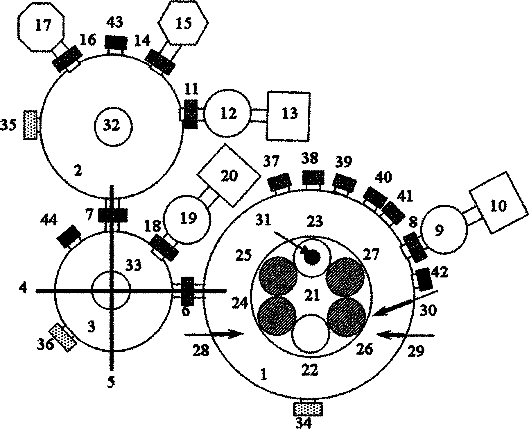
[0039] figure 1 It is a structural schematic diagram (top view) of a multifunctional ion beam sputtering and etching and in-situ physical property analysis system provided by the present invention with a sample exchange vacuum chamber, a six-sub-stage planetary structure sample workpiece table, and three sets of vacuum devices . The names of the components corresponding to the numbers in the figure are: 1 sputtering / etching vacuum chamber, 2 physical property analysis vacuum chamber, 3 sample exchange vacuum chamber, 4 sputtering / etching vacuum chamber and sample exchange vacuum chamber 5. The sample transfer part between the vacuum chamber for physical property analysis and the sample exchange vacuum chamber. 6. The gate...


PUM


Abstract

The invention discloses a multifunctional ion beam sputtering and etching and in-situ physical property analysis system. The system comprises an ion beam sputtering and etching chamber, a physical property analyzing chamber, a sample exchange vacuum cavity, a sputtering sedimentation and etching workpiece stage arranged at the center on the top of the sputtering and etching chamber, an etching ion source arranged at the center on the bottom of the sputtering and etching chamber, two sputtering target stages arranged on the lower part of the sputtering and etching chamber, two sputtering ion source arranged on the middle part of the sputtering and etching chamber, an auxiliary washing ion source arranged on the middle part of the sputtering and etching chamber, and a set of X-ray photoelectron spectroscopy analysis system arranged in the physical property analyzing chamber. The sample exchange vacuum cavity is used for realizing the exchanging and transporting of the sample between thesputtering and etching chamber and the physical property analyzing chamber. The multiple functions are combined in the equipment. The equipment can be used in sputtering sedimentation, etching, polishing and thinning, heat treatment, and sample in-situ physical property analysis of high-quality multi-layer ultra-thin media and metal film materials.

Description

technical field [0001] The invention relates to the technical field of thin film deposition, processing and analysis equipment, in particular to a multifunctional ion beam sputtering and etching and in-situ physical property analysis system. Background technique [0002] Ion beam sputtering deposition (IBSD) is one of the important methods of thin film preparation in semiconductor technology. According to the principle of sputtering, the surface of the target is bombarded with a low-energy focused ion beam, and the sputtered target is deposited on the surface of the substrate and deposited on the surface of the substrate. firmly attached to the substrate surface. The filament in the ion gun generates thermal electrons under high pressure, which ionize argon gas into Ar + , are accelerated under an electric field to form an ion beam. [0003] Reactive ion beam sputtering deposition (RIBD) can be performed under local oxygen pressure or oxygen ion beam bombardment to prepare...

Claims


Application Information

Patent Timeline
Patent Type & Authority Applications(China)
IPC IPC(8): G01N23/00G01B15/02C23C14/46C23F4/04
Inventor 龙世兵刘明谢常青陈宝钦徐连生胡媛
Owner INST OF MICROELECTRONICS CHINESE ACAD OF SCI
Why Eureka
Try Eureka