

Preparation method of thermal-sensitive ceramic sputtered film electrode
A heat-sensitive ceramic and sputtering film technology, which is applied in the field of sputtering to prepare heat-sensitive ceramic electrode films, can solve the problems of low impact current resistance, high production cost, and high cost, and achieve excellent high-temperature welding performance and sputtering film formation The effect of fast speed and low production cost
- Summary
- Abstract
- Description
- Claims
- Application Information
AI Technical Summary
Problems solved by technology
Method used
Image

Examples
preparation example Construction
[0020] The preparation method of the heat-sensitive ceramic sputtering film electrode of the present invention mainly adopts technical steps such as ceramic cleaning, mask mounting, vacuuming, filling with working gas, and sputtering electrode film; the contents of each step are as follows:
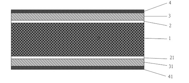
[0021] Ceramic cleaning: The pressed and sintered ceramic substrate 1 should be cleaned before the electrode layer is prepared on its surface to obtain a clean surface; cleaning is divided into rough cleaning, fine, drying, and drying steps; rough cleaning is carried out in a ball mill, and the Put the ceramic substrate 1 in a ball mill filled with running water and wash it for about 15-60 minutes to remove the burrs and heavy pollutants on the surface of the ceramic substrate 1, then put it into tap water and deionized water respectively, and ultrasonically clean it for 10-20 minutes each , and finally centrifugally dried, and dried in an environment of 120°-150°C; the ceramic is BaTiCO ...
Embodiment 1
[0031] Put the 20mm×20mm×4mm PTC heating ceramic body 1 into a ball mill for half an hour, then put it into tap water and deionized water for ultrasonic cleaning 3 times, 20 minutes each time. Then dry at 120°C for 20min;
[0032] Vacuuming: Put the cleaned PTC ceramics in the multi-target magnetron sputtering equipment to vacuumize to make the vacuum degree reach 10 -3 Pa level;
[0033] Filling with working gas: PTC ceramics are placed in the vacuum chamber of the multi-target magnetron sputtering coating machine, and the vacuum chamber is pumped to 8×10 -3 After the Pa vacuum state, then dynamically input inert gas such as Ar into the vacuum chamber to maintain the pressure in the vacuum chamber at 5×10 -1 Pa;
[0034] Sputtering electrode film: The bottom transition layer is sputtered on the front and back surfaces of the ceramic substrate by magnetron sputtering. The material is a Cr film with a thickness of 300nm and an intermediate barrier layer of 300nm. Layer Ag f...
experiment example 2
[0037] The difference between this embodiment and Embodiment 1 lies in the structure of the intermediate barrier layer. In this example, after the bottom electrode is sputtered, the Cr target and the NiCu target are sputtered simultaneously, that is, the structure of the intermediate barrier layer is an alloy of Cr-NiCu; The remaining steps are the same as in Experimental Example 1, and will not be repeated here;
[0038] In this embodiment, the final film layer structure is Cr / CrNiCu / Ag, and the film thicknesses are 300nm / 700nm / 300nm respectively. After testing, the electrode and BaTiO 3The ohmic contact resistance formed by PTC heating ceramics is less than 0.4Ω, the bonding force is greater than 6.4MPa, and the electrode can withstand 350 o C4 seconds of high temperature lead-free solder erosion; after 250 o After aging for 10 hours at C, there is little change in the ohmic contact resistance.
PUM
| Property | Measurement | Unit |
|---|---|---|
| Thickness | aaaaa | aaaaa |
| Thickness | aaaaa | aaaaa |
| Thickness | aaaaa | aaaaa |
Abstract
Description
Claims
Application Information