n-type organic semiconductor materials containing oblique naphthalimide units
What is AI technical title?
AI technical title is built by Patsnap AI team. It summarizes the technical point description of the patent document.
An organic semiconductor and imide technology, applied in the field of n-type semiconductor materials, can solve the problems of lack of high electron mobility, air-stable n-type organic semiconductor materials, and few types
Active Publication Date: 2016-06-29
FUJIAN INST OF RES ON THE STRUCTURE OF MATTER CHINESE ACAD OF SCI
View PDF3 Cites 0 Cited by
Summary
Abstract
Description
Claims
Application Information
AI Technical Summary
This helps you quickly interpret patents by identifying the three key elements:
Image
Click on the blue label to locate the original text in one second.
Reading with bidirectional positioning of images and text.
[0021] Add 0.85 g of 1,5-dicyano-2,6-dimethylnaphthalene and 20 mL of K 2 Cr 2 o 7 (3.56g) and NaOH (0.33g) in water. After the mixture was stirred for half an hour, it was sealed in a stainless steel jar, heated to 220°C and maintained for 10 hours. After cooling, it was filtered, and the filtrate was treated with ether, and the aqueous layer was acidified by adding concentrated hydrochloric acid to obtain a yellow solid (1.06 g, yield 85%). Preparation 2: 1,2,5,6-naphthalene tetracarboxylic anhydride
preparation example 2
[0022] Add 1.0 g of 1,2,5,6-naphthalene tetracarboxylic acid obtained in the previous step into 50 mL of acetic anhydride, stir and reflux in a 100 mL round bottom flask for 3 hours, distill off most of the solvent under reduced pressure, vacuum filter, and the residue After washing with methanol, 0.79 g of product was obtained with a yield of 90%.
preparation example 3
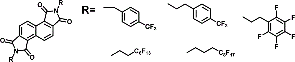
[0023] Preparation Example 3: N, N'-bis(4-(trifluoromethyl)phenyl)-naphthalene-1,2,5,6-bis(dicarboxamide)
[0024]
[0025] The acid anhydride (0.586g, 2.2mmol) obtained in the previous step reaction and excess 4-trifluoromethylbenzylamine (6.6mmol) and zinc acetate (1.54mmol) were added in a 25mL round bottom flask, and 6mL quinoline was added, Heating to above 200°C, stirring and reacting at this temperature for 3 hours. After cooling, vacuum filter, and successively use hot dilute Na 2 CO 3 solution, water, toluene, methanol wash. 1.06 g of crude product were obtained, yield 83%. The further extraction of the product was purified by vacuum sublimation. Elemental analysis: calcdforC, 61.86; H, 2.77; N, 4.81; found: C, 62.03; H, 2.77, N, 4.87. 30 h 16 f 6 N 2 o 4 :582.1, found: 582.1; 1 HNMR (400MHz, CDCl 3 , ppm): δ=4.97(s, 4H), 7.60(s, 8H), 8.12(d, J=8.4Hz, 2H), 9.35(d, J=8.4Hz, 2H).
PUM
Abstract
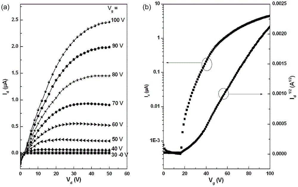
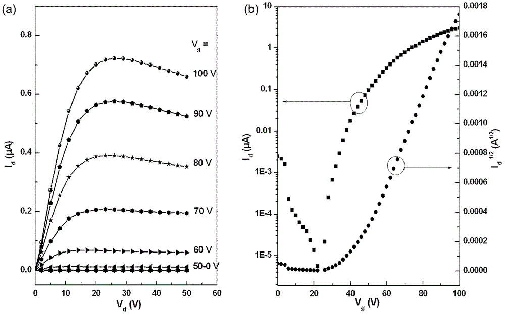
The invention provides an n-type organic semiconductor material containing oblique aromatic naphthalenediimide units, which can be used for organic thin film field effect transistors. This material changes the characteristics of the previous linear naphthalenediimine molecule, which connects the six-membered carboxylateimide ring to the 1, 8 and 4, 5 positions of the naphthalene ring, and changes it to the 1, 2 and 4 positions connected to the naphthalene ring. The 5 and 6 positions form a five-membered ring and a slash type, which can change the charge distribution and electronic energy level of the material molecule. This structure is conducive to the introduction of polymerizable groups at the 3 and 7 positions of the naphthalene ring to synthesize polymers containing oblique aromatic naphthalene diimide units.
Description
technical field [0001] The invention relates to an n-type semiconductor material used in an organic thin film field effecttransistor, in particular to an organic small molecule n-type semiconductor material containing oblique naphthalene cyclodiimide units. Background technique [0002] Field EffectTransistor (Field EffectTransistor, FET) is an active device that uses an electric field to control the conductivity of solid materials, and has become one of the important components in the microelectronics industry. At present, field-effect transistors are close to the natural limit of miniaturization, and the cost is high, which is not conducive to the preparation of large surface area devices. The characteristics of organic field-effect transistors (OFET) can just overcome the above-mentioned shortcomings: wide sources of materials, can be made into flexible devices, can be made into large-area devices, suitable for low-temperature processing, can be processed into films by...
Claims
Application Information
Patent Timeline
Application Date:The date an application was filed.
Publication Date:The date a patent or application was officially published.
First Publication Date:The earliest publication date of a patent with the same application number.
Issue Date:Publication date of the patent grant document.
PCT Entry Date:The Entry date of PCT National Phase.
Estimated Expiry Date:The statutory expiry date of a patent right according to the Patent Law, and it is the longest term of protection that the patent right can achieve without the termination of the patent right due to other reasons(Term extension factor has been taken into account ).
Invalid Date:Actual expiry date is based on effective date or publication date of legal transaction data of invalid patent.
Patent Type & AuthorityPatents(China)
IPC IPC(8): C07D487/04H01L51/30
Inventor郑庆东陈善慈
OwnerFUJIAN INST OF RES ON THE STRUCTURE OF MATTER CHINESE ACAD OF SCI

