Application of tellurium-based composite film as SOI (Semiconductor On Insulator) material and SOI power device

A technology for composite thin films and power devices, which is applied in the fields of semiconductor devices, semiconductor/solid-state device manufacturing, and electrical components. Effects of Voltage and On-Current

Inactive Publication Date: 2013-12-11
CHONGQING UNIV
View PDF1 Cites 0 Cited by
  • Summary
  • Abstract
  • Description
  • Claims
  • Application Information

AI Technical Summary

Problems solved by technology

[0005] For the above-mentioned deficiencies existing in the prior art, the purpose of the present invention is to solve SOI material and directly adopt SiO 2 As an insulating layer, but there will be problems such as incomplete oxidation and affecting the isolation effect of the insulating layer.

Method used


Image

  • Application of tellurium-based composite film as SOI (Semiconductor On Insulator) material and SOI power device
  • Application of tellurium-based composite film as SOI (Semiconductor On Insulator) material and SOI power device

Examples


Embodiment Construction

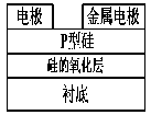
[0016] Application of a tellurium-based composite thin film as an insulating layer of an SOI device, the tellurium-based composite thin film contains SiO 2 The particles are embedded with TeO 2 and / or Te to form Te / TeO 2 - SiO 2 Composite thin film structure (for its preparation method refer to CN101838112A). Through experimental research, the resistivity of tellurium-based composite films reaches 1200Ω·m, the relative permittivity is less than 3.9, and the band gap is above 3.4eV, which proves that tellurium-based composite films have high resistance characteristics, small relative permittivity, and large Bandgap width, high critical breakdown electric field, and high electron mobility have become ideal insulating materials for SOI devices.

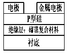
[0017] The tellurium-based composite thin film is applied to the SOI device, and the SOI structure Schottky diode device with the tellurium-based composite thin film as the silicon insulating layer is prepared. Such as figure 2 As ...


PUM

PropertyMeasurementUnit
electrical resistivityaaaaaaaaaa
relative permittivityaaaaaaaaaa

Abstract

The invention discloses an application of a tellurium-based composite film as an SOI (Semiconductor on Insulator) material. The tellurium-based composite film is of a composite film structure formed in a manner that TeO2 and / or Te are embedded among SiO2-containing particles to form Te / TeO2-SiO2. The tellurium-based composite film is applied to an SOI device, and a Schottky diode device which is of an SOI structure taking the tellurium-based composite film as a silicon insulation layer is manufactured. The test research proves that the tellurium-based composite film has the characteristics of high resistance property, smaller dielectric constant, high forbidden band width, high critical breakdown electrical field, high electron mobility and the like, and becomes an ideal insulation material for manufacture of the SOI device. According to the invention, the problem on the SOI insulation layer is solved, and the application field of the tellurium-based composite film is developed.

Description

technical field [0001] The invention relates to the application of a tellurium-based composite thin film as an insulating layer of an SOI device, which belongs to the technical field of semiconductor high-frequency and high-power devices, and particularly relates to the technical field of SOI (Semiconductor On Insulator) power devices. Background technique [0002] SOI material is the abbreviation of new silicon-based integrated circuit material. This type of material is developed to meet the needs of the control of aerospace electronics, missiles and other weapon systems and satellite electronic systems. SOI materials have the following outstanding advantages: 1. Low power consumption; 2. Low turn-on voltage; 3. High speed; 4. Improve integration; 5. Fully compatible with existing integrated circuits and reduce process procedures; 6. High temperature resistance; 7. Anti-irradiation to reduce software errors. These advantages make SOI technology have an extremely wide appl...

Claims


Application Information

Patent Timeline
Patent Type & Authority Patents(China)
IPC IPC(8): H01L21/762H01L29/06H01L29/872
Inventor 辜敏甘平鲜晓东
Owner CHONGQING UNIV
Why Eureka
Try Eureka