Preparation method of submicron-grade graph on sapphire substrate

A sapphire substrate, sub-micron technology, applied in electrical components, circuits, semiconductor devices, etc., can solve the problems affecting the performance of nitride LED devices, lattice constant mismatch and thermal expansion coefficient differences.

Inactive Publication Date: 2012-06-27
南京大学扬州光电研究院
View PDF4 Cites 14 Cited by
  • Summary
  • Abstract
  • Description
  • Claims
  • Application Information

AI Technical Summary

Problems solved by technology

However, there is a large lattice constant mismatch and thermal expansion coefficient difference between the sapphire substrate and the nitride epitaxial layer, resulting in the threading disloc

Method used


Image

  • Preparation method of submicron-grade graph on sapphire substrate
  • Preparation method of submicron-grade graph on sapphire substrate
  • Preparation method of submicron-grade graph on sapphire substrate

Examples


Embodiment 1

[0030] Step 1: Deposit a layer of 10nm silicon dioxide on the sapphire substrate as a photoresist adhesion layer for fine lithography on the sapphire substrate.

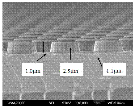
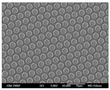
[0031] Step 2: Prepare a photoresist pattern mask layer with cylindrical holes with a diameter of 2.5 μm and an interval of 1 μm on the sapphire substrate prepared in step 1 by conventional photolithography technology.

[0032]Step 3: A four-layer metal structure consisting of a 10nm Ti layer, a 50nm Ni layer, a 10nm Al layer, and a 100nm Ni layer is sequentially evaporated on the sapphire substrate made in step 2 using vacuum evaporation equipment, as an etched sapphire substrate metal mask. Wherein, the thickness of each Ti layer and Al layer is 10 nm and 15 nm respectively, and the thickness of each metal Ni layer is 50 nm.

[0033] Step 4: Sonicate the sapphire substrate prepared in step 3 by immersing it in boiling acetone for 3 minutes to 15 minutes to carry out the photoresist stripping process, and then rins...

Embodiment 2

[0042] Step 1: Deposit a layer of 200nm silicon dioxide on the sapphire substrate as a photoresist adhesion layer for fine lithography on the sapphire substrate.

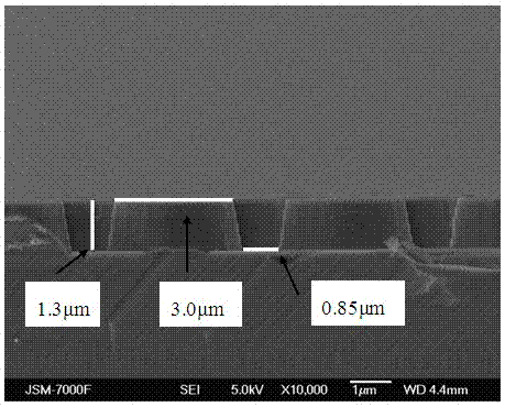
[0043] Step 2: Prepare a photoresist pattern mask layer with cylindrical holes with a diameter of 3 um and an interval of 1 um on the sapphire substrate produced in step 1 by conventional photolithography technology.

[0044] Step 3: Use vacuum evaporation equipment to sequentially vapor-deposit a four-layer metal structure of 10nm Al layer, 100nm Ni layer, 10nm Au layer, and 100nm Ni layer on the sapphire substrate prepared in step 2, as the metal for etching the sapphire substrate mask,

[0045] Wherein, the thicknesses of the Au layer and the Al layer are 20nm and 35nm respectively, and the thickness of each metallic Ni layer is 5nm.

[0046] Step 4: Immerse the sapphire substrate prepared in step 3 into boiling acetone for 3 minutes to 15 minutes and perform the photoresist stripping process, and then rinse it ...


PUM

PropertyMeasurementUnit
Thicknessaaaaaaaaaa
Thicknessaaaaaaaaaa
Diameteraaaaaaaaaa

Abstract

The invention relates to a preparation method of a submicron-grade graph on a sapphire substrate, which belongs to the technical field of semiconductors and comprises the following steps of: firstly depositing a photoresist-adhering layer on the sapphire substrate, then carrying out the ultrasonic processing of the sapphire substrate in acetone through photoetching and vapor deposition, and cleanly flushing by adopting deionized water; then placing the sapphire substrate into a hydrochloric-acid aqueous solution for heating to ultrasonically remove a metallic mask layer after being etched by adopting an inductively-coupled plasma dry method, flushing with the deionized water, and then placing the sapphire substrate into dilute hydrofluoric acid or a heated phosphoric-acid solution to remove the photoresist-adhering layer; and finally placing the substrate into the acetone and alcohol for ultrasonic processing, and then cleanly flushing with the deionized water. The preparation method of the submicron-grade graph on the sapphire substrate has the advantages of low manufacturing cost, easiness in operation and high finished-product rate, can be used for the epitaxial growth of low-dislocation-density high-crystal-quality nitrides and can be used for producing the substrate material of a nitride-semiconductor light-emitting diode with higher light-emitting efficiency.

Description

technical field [0001] The invention belongs to the technical field of semiconductors, in particular to a preparation method for preparing submicron patterns on a sapphire substrate by means of ultraviolet lithography technology. Background technique [0002] Gallium nitride (GaN), aluminum nitride (AlN), indium nitride (InN) and other three-group nitride wide bandgap semiconductor material systems and related ternary and quaternary alloys, due to their wide bandgap (from 0.6 The infrared region of eV has been covered to the deep ultraviolet region of 6.1eV) and excellent optical and electrical properties, in the field of optoelectronic devices such as light-emitting diodes (LEDs) and lasers (LDs) in blue, green, ultraviolet (UV) and deep ultraviolet band Has a wide range of applications. Due to the lack of homoepitaxial substrates, most of the substrate materials prepared by nitride-based LED devices use sapphire substrates, SiC substrates or Si substrates. Among them, sap...

Claims


Application Information

Patent Timeline
IPC IPC(8): H01L33/00
Inventor 陈鹏王栾井宋雪云谭崇斌徐峰徐洲吴真龙高峰邵勇
Owner 南京大学扬州光电研究院
Why Eureka
Try Eureka