Terahertz GaN Gunn diode based on SiC substrate and manufacturing method thereof

A Gunn diode, terahertz technology, applied in the field of microelectronics, can solve the problem of high dislocation density at the interface of the heterojunction, and achieve the elimination of piezoelectric polarization effect, high power and frequency, and improve the characteristics of high frequency and high power. Effect

Active Publication Date: 2012-06-27
云南凝慧电子科技有限公司
View PDF4 Cites 15 Cited by
  • Summary
  • Abstract
  • Description
  • Claims
  • Application Information

AI Technical Summary

Problems solved by technology

Although this structure has significantly improved the performance of the device, there are still some problems.
Because there is a difference in lattice constant between AlGaN and GaN, the piezoelectric polarization effect will be generated at the interface, and the dislocation density at the heterojunction interface is high

Method used


Image

  • Terahertz GaN Gunn diode based on SiC substrate and manufacturing method thereof
  • Terahertz GaN Gunn diode based on SiC substrate and manufacturing method thereof
  • Terahertz GaN Gunn diode based on SiC substrate and manufacturing method thereof

Examples


Embodiment 1

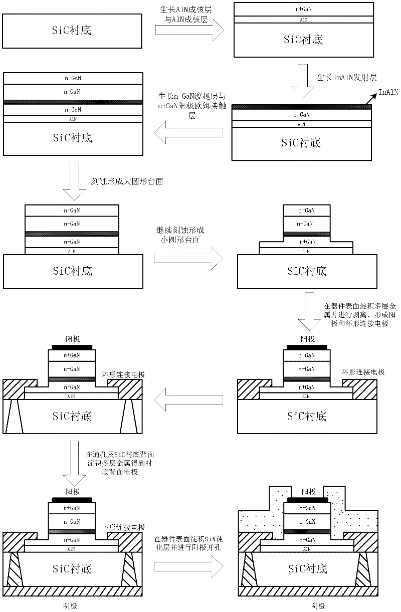
[0037] The steps of making the terahertz GaN Gunn diode in the present invention are as follows:

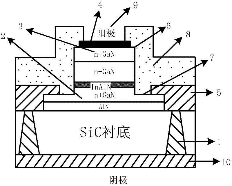
[0038] Step 1: Select a 4H-SiC semi-insulating SiC substrate with a diameter of 2 inches, and thin the back surface to a substrate thickness of 150 μm.

[0039] Step 2: Using trimethylaluminum and high-purity nitrogen as aluminum and nitrogen sources on MOCVD, a low-temperature AlN nucleation layer with a thickness of 30 nm is first grown on the SiC substrate, and the growth conditions are as follows: the temperature is 600 ° C, The pressure was 40 Torr.

[0040] Step 3, continue to adopt the MOCVD process, use triethylgallium and high-purity nitrogen gas as the gallium source and nitrogen source respectively, and silane gas as the n-type doping source, and epitaxially grow a layer with a doping concentration of 1.0× on the AlN nucleation layer 10 18 cm -3 , n with a thickness of 0.5 μm + The GaN cathode ohmic contact layer is grown under the following conditions: a temperatu...

Embodiment 2

[0051] The steps of making the terahertz GaN Gunn diode in the present invention are as follows:

[0052] Step 1, select a 6H-SiC conduction-type n-type SiC substrate with a diameter of 3 inches, and a doping concentration of 2.0×10 18 cm -3 , the back side is thinned to a substrate thickness of 200 μm.

[0053] Step 2: Using trimethylaluminum and high-purity nitrogen as aluminum and nitrogen sources, a low-temperature AlN nucleation layer with a thickness of 50nm is grown on the SiC substrate by using a MOCVD process with a temperature of 600°C and a pressure of 40 Torr.

[0054] Step 3, continue to use the MOCVD process, under the process conditions of a temperature of 1000 ° C and a pressure of 40 torr, triethylgallium and high-purity nitrogen gas are used as the gallium source and nitrogen source respectively, and silane gas is used as the n-type doping source. An epitaxial growth layer on the AlN nucleation layer with a doping concentration of 2.0×10 18 cm -3 , n with...

Embodiment 3

[0076] The steps of making the terahertz GaN Gunn diode in the present invention are as follows:

[0077] In step A, a 4H-SiC semi-insulating SiC substrate with a diameter of 3 inches is selected, and the back surface is thinned to a substrate thickness of 150 μm.

[0078] Step B, make n + GaN cathode ohmic contact layer:

[0079] B1) First, using trimethylaluminum and high-purity nitrogen as the aluminum source and nitrogen source respectively, a low-temperature AlN nucleation layer with a thickness of 40 nm is grown on the SiC substrate by MOCVD process, and the growth conditions are as follows: the temperature is 600 ° C, The pressure is 40 torr;

[0080] B2) Under the process conditions of a temperature of 1000°C and a pressure of 40 Torr, continue to use the MOCVD process, using triethylgallium and high-purity nitrogen as the gallium source and nitrogen source respectively, and silane gas as the n-type doping source. On the nucleation layer, epitaxially grow a layer wi...


PUM


Abstract

The invention discloses a terahertz GaN Gunn diode based on an SiC substrate and a manufacturing method thereof, which are used for mainly solving the problems of low output power, poor heat radiation performance and the like in the traditional Gunn device structure. The diode respectively comprises the SiC substrate, an AlN nucleating layer, an n+GaN ohmic contact layer, an electron emitting layer, an n-GaN active layer and an n+GaN ohmic contact layer from bottom to top and is characterized in that the electron emitting layer is made of an InAlN material with 14-22% of an In component and has the thickness of 80-200 nm; a through hole (1) is etched in the SiC substrate; metals Ti/Al/Ni/Au are deposited at the bottom of the substrate; and the metals are connected with an annular electrode (5) through the through hole, so that a longitudinal device structure is formed. The terahertz GaN Gunn diode disclosed by the invention is capable of eliminating a piezoelectric polarization effect and obviously reducing interface dislocation and the length of a Dead Zone, has the advantages of high output power and working frequency, and is applied to working in terahertz frequency bands.

Description

technical field [0001] The invention belongs to the field of microelectronics and relates to a Gunn diode structure of wide bandgap semiconductor GaN material, which can be used in high-frequency, high-power and other fields. Background technique [0002] Wide bandgap semiconductor materials represented by GaN and SiC are new semiconductor materials that have developed rapidly in the past ten years following the first-generation semiconductor materials represented by semiconductor Si and the second-generation semiconductor materials represented by GaAs. GaN-based semiconductor materials have excellent characteristics such as wide bandgap, direct bandgap, high electron drift velocity, high thermal conductivity, high voltage resistance, high temperature resistance, corrosion resistance, radiation resistance, and high heterojunction two-dimensional electron gas concentration. The field of wave high-power electronic devices has received widespread attention. [0003] As an emer...

Claims


Application Information

Patent Timeline
Patent Type & Authority Applications(China)
IPC IPC(8): H01L47/02
Inventor 杨林安毛伟何寒冰郝跃
Owner 云南凝慧电子科技有限公司
Why Eureka
Try Eureka