

Preparation method for cuprous oxide micron/nano crystal with controllable morphology
A technology of cuprous oxide and nanocrystals, applied in the direction of copper oxide/copper hydroxide, nanotechnology, etc., can solve the problems of environmental pollution, high cost of micro/nano cuprous oxide, etc., and achieve low preparation cost, cheap raw material price, and Source Rich Effects
- Summary
- Abstract
- Description
- Claims
- Application Information
AI Technical Summary
Problems solved by technology
Method used
Image

Examples
specific Embodiment approach 1
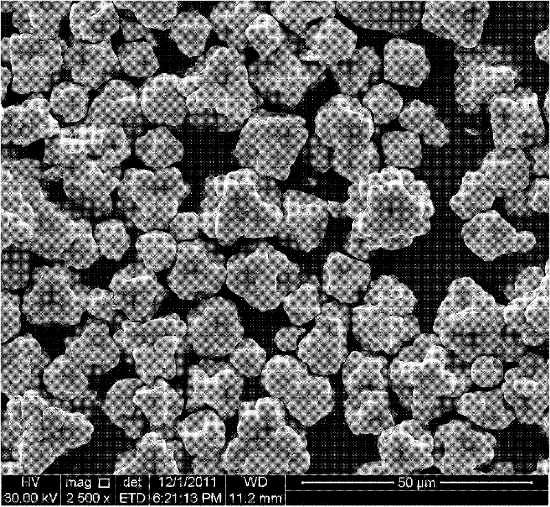
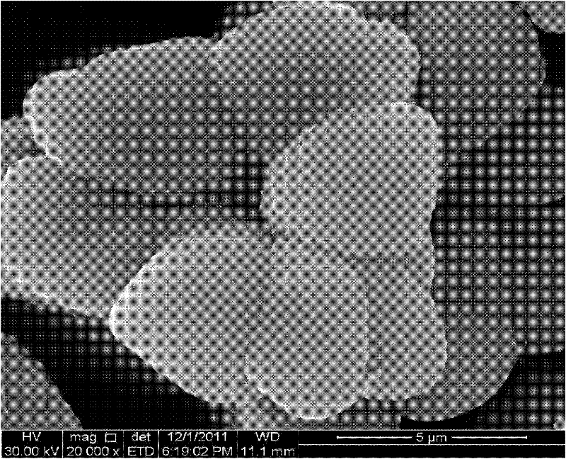
[0017] Specific embodiment 1: The preparation method of the shape-controllable cuprous oxide micro / nano crystal in this embodiment is carried out according to the following steps:
[0018] Step 1. Add 0.002-0.1mol copper salt into 15mL-30mL ultrapure water, stir with a magnetic stirrer at a rate of 500-1000r / min until the copper salt is completely dissolved, and then set the molar ratio of copper ion to lactic acid as 1: (5-20) into lactic acid, continue to stir for 30-60 minutes, then adjust the pH value to 7.0-13.0 with alkaline solution, then cool to 25°C and set the volume to 100mL, measure the pH value, and obtain solution A;
[0019] Step 2. Then move the solution A to the cleaned hydrothermal reaction kettle, close the reaction kettle, put the hydrothermal reaction kettle into the oven, adjust the temperature of the oven to 50-200°C, keep it warm for 2-48 hours and then cool it down naturally to room temperature, take it out and wash it with ultrapure water for three ti...
specific Embodiment approach 2
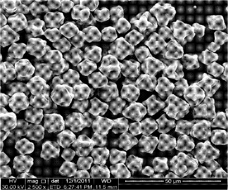
[0020] Embodiment 2: This embodiment differs from Embodiment 1 in that: Step 1 adds 0.03-0.08 mol of copper salt into 20 mL of ultrapure water. Other steps and parameters are the same as those in Embodiment 1 or Embodiment 2.
specific Embodiment approach 3
[0021] Embodiment 3: The difference between this embodiment and Embodiment 1 or 2 is that the molar ratio of copper ions to lactic acid in Step 1 is 1: (6-15). Other steps and parameters are the same as those in Embodiment 1 or Embodiment 2.
PUM
 Abstract
Description
Claims
Application Information