Check patentability & draft patents in minutes with Patsnap Eureka AI!

Split-gate flash memory unit and manufacturing method thereof

The technology of a flash memory unit and manufacturing method is applied in semiconductor/solid-state device manufacturing, electrical components, information storage, etc., which can solve the problems of device miniaturization limitation, large programming voltage of split-gate flash memory unit, etc., and achieve the advantages of device size, overcome Effect of short channel effect and low power consumption

Active Publication Date: 2012-07-18
SHANGHAI HUAHONG GRACE SEMICON MFG CORP
View PDF6 Cites 0 Cited by
  • Summary
  • Abstract
  • Description
  • Claims
  • Application Information

AI Technical Summary

Problems solved by technology

[0005] However, the programming voltage of existing split-gate flash memory cells is relatively high, and the miniaturization of devices is limited
In the Chinese patent application whose publication number is CN1881592A, a kind of storage device with SONOS (silicon oxide nitride oxide) structure is proposed, but the above-mentioned problems are still not solved

Method used


Image

  • Split-gate flash memory unit and manufacturing method thereof
  • Split-gate flash memory unit and manufacturing method thereof
  • Split-gate flash memory unit and manufacturing method thereof

Examples


Embodiment Construction

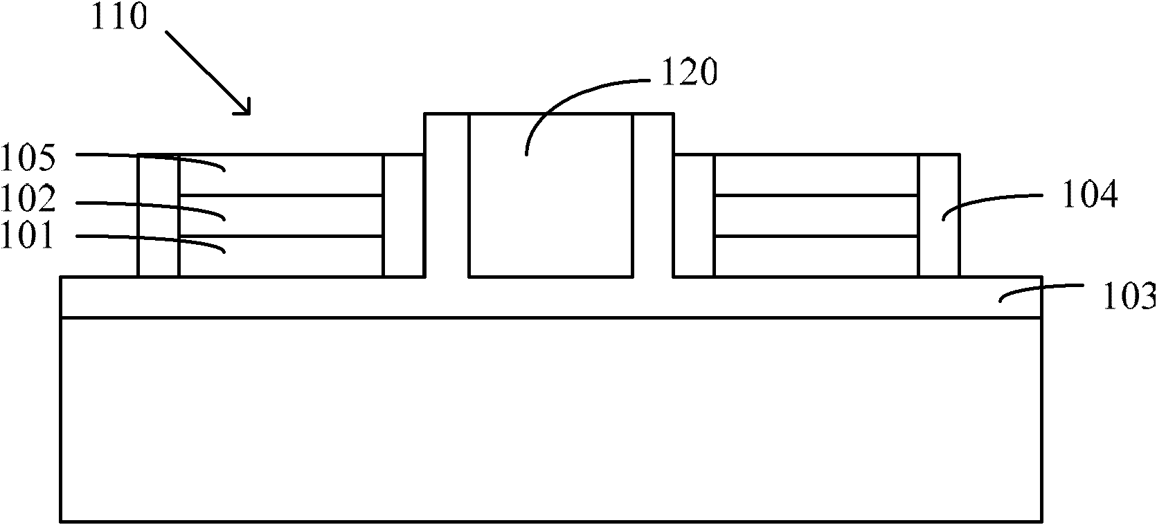
[0032] It can be seen from the background art that the programming voltage of the existing split-gate flash memory cell is relatively high, and the miniaturization of the device is limited. The inventors of the present invention found that the existing split-gate flash memory unit uses polysilicon as the storage medium, which uses the same polysilicon as the general gate, so it can be well compatible with the traditional process, but due to its conductivity, in order to ensure The data retention of the storage device must ensure that there are no oxide defects, so the thickness of the tunnel oxide layer cannot be further reduced (generally greater than 70 angstroms), which is not conducive to the reduction of the operating voltage, resulting in reduced device size. limit. After further research, the inventor provides a split-gate flash memory unit and a manufacturing method thereof in the present invention.

[0033] figure 2 It is a schematic flow chart of the method for ma...


PUM

PropertyMeasurementUnit
Widthaaaaaaaaaa
Thicknessaaaaaaaaaa
Thicknessaaaaaaaaaa

Abstract

The invention discloses a manufacturing method of a split-gate flash memory unit. The method comprises the following steps of: providing a substrate, wherein the substrate comprises at least two first regions and a second region positioned between the two first regions, and a tunneling layer, a silicon nitride layer, a barrier layer and a control grid are formed in sequence on the surface of the substrate in the first regions; forming a groove on the substrate in the second region; forming a spacer medium layer on the surface of the groove, and forming word lines which are filled up the groove, and of which the thicknesses are larger than the depth of the groove; and forming source regions and drain regions for the tunneling layer and the barrier layer in the substrate in the first regions. Correspondingly, the invention further provides a split-gate flash memory unit formed by using the method. According to the split-gate flash unit and the manufacturing method thereof provided by the invention, data are stored by using locally separated charges, so that miniaturization of a device is realized; and moreover, by adopting the split-gate flash unit and the manufacturing method thereof provided by the invention, the programming voltage can be lowered, power consumption is lowered, and the short-channel effect can be overcome.

Description

technical field [0001] The invention relates to the field of semiconductor technology, in particular to a split-gate flash memory unit and a manufacturing method thereof. Background technique [0002] In the current semiconductor industry, integrated circuit products can be mainly divided into three types: analog circuits, digital circuits and digital / analog hybrid circuits, among which storage devices are an important type of digital circuits. Among storage devices, the development of flash memory (flash memory for short) is particularly rapid in recent years. The main feature of flash memory is that it can keep stored information for a long time without power on; and it has the advantages of high integration, fast access speed, easy erasing and rewriting, etc., so it has been widely used in many fields such as microcomputer and automatic control. a wide range of applications. [0003] The standard physical structure of flash memory is called a flash cell (bit). The stru...

Claims


Application Information

Patent Timeline
IPC IPC(8): H01L21/8247H01L27/115H01L29/51H01L29/06H01L29/10G11C16/04
Inventor 曹子贵
Owner SHANGHAI HUAHONG GRACE SEMICON MFG CORP
Features
  • R&D
  • Intellectual Property
  • Life Sciences
  • Materials
  • Tech Scout
  • Unparalleled Data Quality
  • Higher Quality Content
  • 60% Fewer Hallucinations
Learn More