Small ultrawide band antenna with trapped wave characteristic

A technology of ultra-wideband antenna and notch characteristics, which is applied in the field of ultra-wideband wireless communication system and small ultra-wideband antenna. Simple antenna structure and easy production

Active Publication Date: 2012-07-25
杭州平治信息技术股份有限公司
View PDF7 Cites 26 Cited by
  • Summary
  • Abstract
  • Description
  • Claims
  • Application Information

AI Technical Summary

Problems solved by technology

Another example is the patent application number 201020531935.X, and the Chinese patent titled "Ultra-Wideband Antenna with Notch Characteristic" proposes a UWB antenna with dual notch characteristics. The antenna consists of a microstrip The feeding rectangular radiating unit and the ground plane of the coplanar waveguide form two notched bands of 3.8GHz-6GHz and 7.5GHz-9GHz by etching double U-shaped slots and rectangular slots on the radiating unit and the floor respectively, but this The bandwidth of the notch frequency band in the invention is too wide, far beyond the frequency range of the interference signal, which undoubtedly leads to the reduction of the working frequency band of the ultra-wideband antenna itself
Another example is the document "Planar Ultrawideband Antennas With Multiple Notched Bands Based on Etched Slots on the Patch and / or Split Ring Resonators on the Feed Line, Yan Zhang, Wei Hong, Chen Yu, Zhen-Qi Kuai, Yu-Dan Don, and Jian -Yi Zhou, I EEE TRANSACTIONS ON ANTENNAS AND PROPAGATION, VOL.56, NO.9, SEPTEMBER2008″ designed an ultra-wideband antenna with three notch characteristics, and the radiation element of the antenna is a microstrip-fed circle Shaped monopole, by loading 3 pairs of open-loop resonators of different sizes on both sides of the feeder to form notches in the 2.24GHz-2.62GHz, 3.78GHz-4.03GHz and 5.94GHz-6.4GHz frequency bands, but the antenna uses 6 An open-loop resonator, the antenna is large in size, and the useful frequency band between the 5.2GHz and 5.8GHz frequency bands is also filtered out, resulting in a waste of frequency bands

Method used


Image

  • Small ultrawide band antenna with trapped wave characteristic
  • Small ultrawide band antenna with trapped wave characteristic
  • Small ultrawide band antenna with trapped wave characteristic

Examples


Embodiment 1

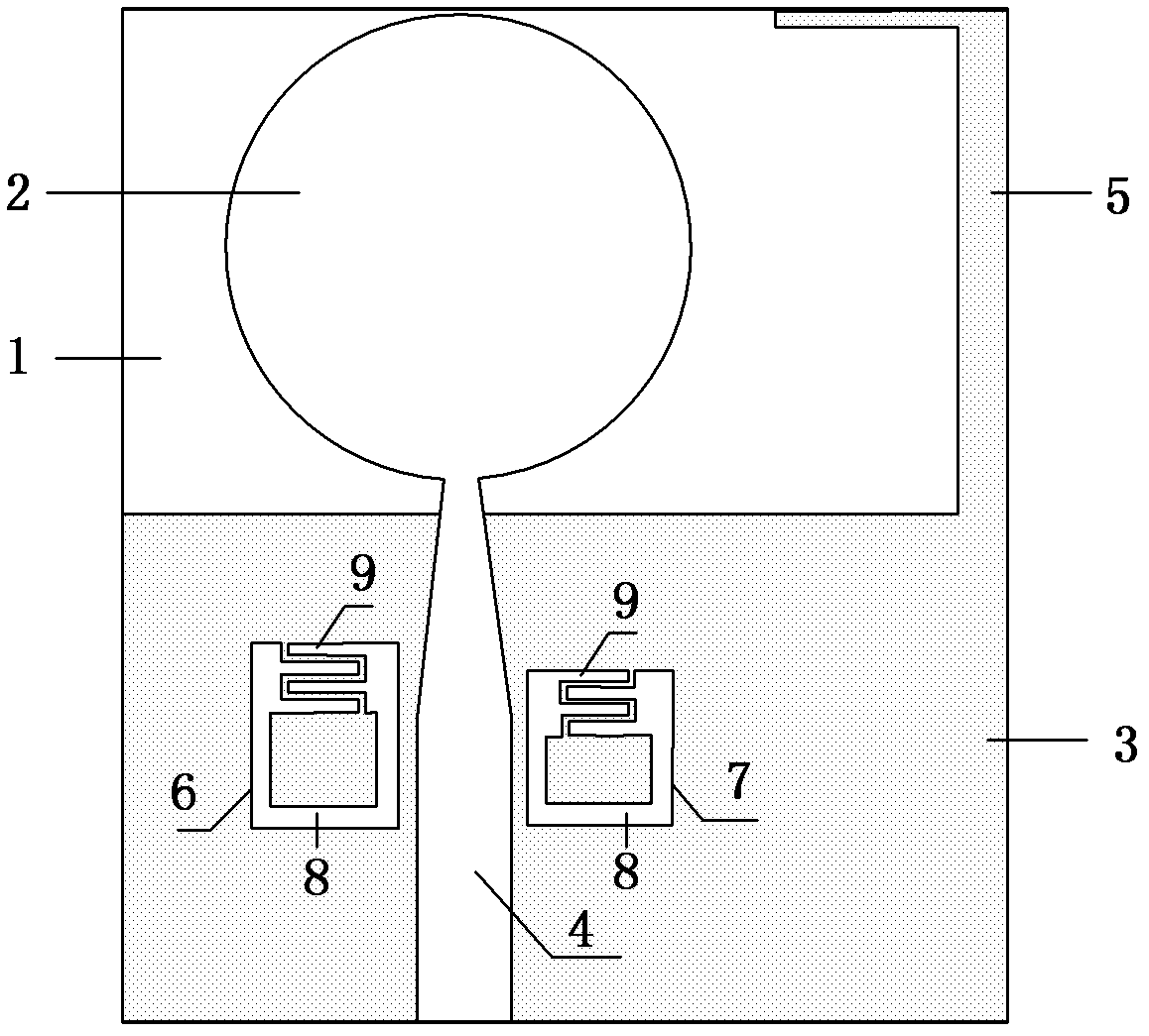
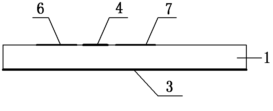
[0037] see figure 1 with figure 2 , the ultra-wideband antenna of the present invention includes: a dielectric substrate 1, a radiating element 2, a metal floor, a microstrip feeder 4, and two interdigitated capacitively loaded resonant rings 6 and 7, the radiating element 2, a microstrip feeder 4, and two The interdigitated capacitively loaded resonant rings 6 and 7 are printed on the upper surface of the dielectric substrate 1 , and the radiation unit 2 adopts a circular patch, and the radiation unit 2 is connected to the upper part of the microstrip feeder 4 . The microstrip feeder 4 is composed of a microstrip line with a characteristic impedance of 50 ohms and a gradient microstrip line with a characteristic impedance linearly changing from 50 ohms to R ohms. The value of R is 60-90 ohms. By adjusting the size of R, The impedance matching characteristics of the antenna in the working frequency band can be optimized. In this embodiment, the value of R is 75 ohms. The rad...

Embodiment 2

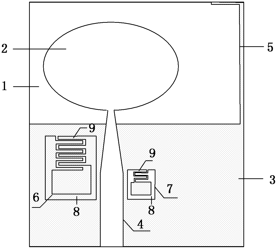
[0044] see image 3 , the radiating unit 2 of the UWB antenna in this embodiment is an elliptical patch, and the other structures are the same as the UWB antenna in Embodiment 1, and the relationship between each structure is also the same as that of the UWB antenna in Embodiment 1. In this embodiment, the microstrip feeder 4 is composed of a microstrip line with a characteristic impedance of 50 ohms and a tapered microstrip line with a linear gradient from 50 ohms to R ohms, where R is 75 ohms, and the radiation unit 2 and the microstrip feeder 4 is located on the left side of the central axis of the dielectric substrate 1, and the distance from the central axis of the dielectric substrate 1 is 2 mm.

[0045] In this embodiment, the inverted L-shaped 5 is located on the right side of the central axis of the dielectric substrate 1, and the minimum operating frequency of the antenna is 3.16 GHz. The size of the inverted L-shaped 5 is: the length of the horizontal branch is 2 mm...

Embodiment 3

[0049] see Figure 4 , the radiation unit 2 of the ultra-wideband antenna in this embodiment is a rectangular patch, the radiation unit 2 and the microstrip feeder 4 are located on the right side of the central axis of the dielectric substrate 1, and the distance from the central axis of the dielectric substrate 1 is 2 mm, in an inverted L shape 5 is located on the left side of the central axis of the dielectric substrate 1, and the rest of the structure is the same as the UWB antenna in Embodiment 1, and the relationship between each structure is the same as that of the UWB antenna in Embodiment 1. In this embodiment, the microstrip feeder 4 It consists of a microstrip line with a characteristic impedance of 50 ohms and a tapered microstrip line with a characteristic impedance linearly changing from 50 ohms to R ohms, and R is 75 ohms.

[0050] The minimum operating frequency of the antenna in this embodiment is 2.93 GHz, and the size of the inverted L-shaped 5 is: the length...


PUM


Abstract

The invention discloses a small ultrawide band antenna with a trapped wave characteristic. The small ultrawide band antenna consists of a dielectric substrate (1) and metal coating layers positioned on the upper surface and the lower surface of the dielectric substrate (1), wherein a radiation unit (2), a microstrip feeder (4) and interdigital capacitance loading resonance rings (6) and (7) are arranged on the upper surface of the dielectric substrate; the microstrip feeder (4) consists of a microstrip line with characteristic impedance of 50 ohms and a microstrip line with characteristic impedance which is gradually changed linearly from 50 ohms; the two interdigital capacitance loading resonance rings (6) and (7) with different sizes are printed on two sides of the microstrip feeder and used for forming a trapped wave frequency band; and a metal floor consists of a rectangle (3) and a reversed L shape (5) and is printed on the lower surface of the dielectric substrate (1). The working frequency band of the antenna covers 3.1 to 10.6 GHz; interference signals of a plurality of narrowstrip frequency bands can be filtered as required by adjusting relevant parameters, and available frequency bands are retained; and the antenna has the advantages of wide frequency band, narrow attenuation band, miniaturization and strong anti-interference capacity.

Description

technical field [0001] The invention belongs to the field of antennas, in particular to a small ultra-wideband antenna with notch characteristics, which is applied to an ultra-wideband wireless communication system. Background technique [0002] Ultra-wideband UWB technology is a new type of wireless communication technology. It has the characteristics of high transmission rate, low power consumption, and simple system structure. It meets the needs of high-speed communication development and has been widely used. As a key component of UWB communication system, the characteristics of UWB antenna will directly affect the transmission performance of the system, so its research and design are of great significance. In 2002, the US Federal Communications Commission (FCC) approved 3.1-10.6GHz as the working frequency band of the ultra-wideband system, and there are inevitably some narrow-band interference signals, such as the wireless local area network WLAN in the frequency bands...

Claims


Application Information

Patent Timeline
Patent Type & Authority Applications(China)
IPC IPC(8): H01Q1/48H01Q1/50H01Q1/38
Inventor 翟会清李桐李桂红李龙梁昌洪
Owner 杭州平治信息技术股份有限公司
Why Eureka
Try Eureka