High-energy-storage density dielectric material and preparation method thereof

A technology of high energy storage density and dielectric materials, applied in the field of high energy storage density dielectric materials and their preparation, can solve the problems of reducing composite materials, brittleness, poor mechanical properties, etc., and achieve the effect of avoiding brittleness

Inactive Publication Date: 2012-08-08
SHANGHAI SECOND POLYTECHNIC UNIVERSITY
View PDF4 Cites 9 Cited by
  • Summary
  • Abstract
  • Description
  • Claims
  • Application Information

AI Technical Summary

Problems solved by technology

[0007] The invention discloses a high energy storage density dielectric material and a preparation method thereof, which aims at overcoming the disadvantages of brittleness and poor mechanical properties in the preparation of high energy storage density dielectric materials by ceramic filling polymers; compare

Method used


Image

  • High-energy-storage density dielectric material and preparation method thereof
  • High-energy-storage density dielectric material and preparation method thereof
  • High-energy-storage density dielectric material and preparation method thereof

Examples


Embodiment 1

[0028] (1) Disperse 0.02 g of nickel-containing carbon nanotubes in 100 ml of DMF solvent, stir on a mechanical stirrer for 1 h, and then put them into an ultrasonic apparatus for ultrasonic treatment for 1 h.

[0029] (2) Dissolve 1.98g of polyvinylidene fluoride in 50ml of DMF solvent, then pour the stirred and ultrasonically treated nickel-containing carbon nanotube solution into the polyvinylidene fluoride solution, and continue to stir on a magnetic stirrer for 1h.

[0030] (3) Pour the obtained complex solution into a petri dish, and dry the solvent in an oven at 100° C. until the inclined petri dish can just flow;

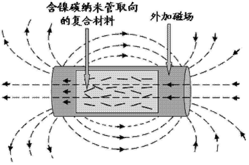
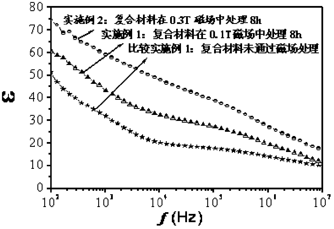
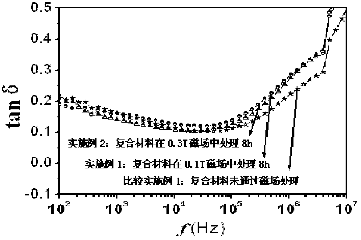
[0031] (4) Place the composite in a 0.1T magnetic field for 8 hours and then dry the solvent in an oven at 100°C to obtain a composite film;

[0032] (5) Cut the composite film and put it into a mold, put it on a hot press at 180° C. and 18 MPa constant pressure for 10 minutes, and press it into a disc sample with a thickness of 1 mm and a diameter of 12 mm....

Embodiment 2

[0035] (1) Disperse 0.02 g of nickel-containing carbon nanotubes in 100 ml of DMF solvent, stir on a mechanical stirrer for 1 h, and then put them into an ultrasonic apparatus for ultrasonic treatment for 1 h.

[0036] (2) Dissolve 1.98g of polyvinylidene fluoride in 50ml of DMF solvent, then pour the stirred and ultrasonically treated nickel-containing carbon nanotube solution into the polyvinylidene fluoride solution, and continue to stir on a magnetic stirrer for 1h.

[0037] (3) Pour the obtained complex solution into a petri dish, and dry the solvent in an oven at 100° C. until the inclined petri dish can just flow;

[0038] (4) Place the composite in a 0.3T magnetic field for 8 hours and then dry the solvent in an oven at 100°C to obtain a composite film;

[0039](5) Cut the composite film and put it into a mold, put it on a hot press at 180° C. and 18 MPa constant pressure for 10 minutes, and press it into a disc sample with a thickness of 1 mm and a diameter of 12 mm. ...

Embodiment 3

[0042] (1) Disperse 0.1 g of nickel-containing carbon nanotubes in 100 ml of DMF solvent, stir on a mechanical stirrer for 3 h, and then put them into an ultrasonic apparatus for ultrasonic treatment for 1 h.

[0043] (2) Dissolve 1.9 g of polyvinylidene fluoride in 50 ml of DMF solvent, then pour the stirred and ultrasonically treated nickel-containing carbon nanotube solution into the polyvinylidene fluoride solution, and continue stirring on a magnetic stirrer for 1 h.

[0044] (3) Pour the obtained complex solution into a petri dish, and dry the solvent in an oven at 80° C. until the inclined petri dish can just flow;

[0045] (4) Place the composite in a 0.1T magnetic field for 5 hours and then dry the solvent in an oven at 80°C to obtain a composite film;

[0046] (5) Cut the composite film and stack it into a mold, press on a hot press at 160° C. and 20 MPa constant pressure for 10 minutes, and press it into a disc sample with a thickness of 1 mm and a diameter of 12 mm...


PUM

PropertyMeasurementUnit
Diameteraaaaaaaaaa

Abstract

Provided is a preparation method of a high-energy-storage density dielectric material. The preparation method comprises firstly dispersing magnetic carbon nanotubes into dimethyl formamide (DMF) solvent for mechanical mixing for 1-3 hours, and performing ultrasonic processing for 1 hour to obtain carbon nanotube solution; independently dissolving ferroelectric polymers into the DMF solvent, and then pouring the prepared carbon nanotube solution into ferroelectric polymer solution for continuous mixing for 1 hour; pouring the compound solution into a glass culture dish made of non-magnetic permeability materials, and drying solvent in the compound solution in a dryer at the temperature of 80-100 DEG C until the compound can only flow when the culture dish inclines; placing the compound to a 0.1-0.5 T magnetic field for standing for 5-10 hours, and continuously drying the compound after being taken out in the dryer at the temperature of 80-100 DEG C to obtain a compound film of the carbon nanotubes solidified in the polymers; cutting the compound film and placing the cut compound film into a mould in an overlaying mode, and pressing the compound films into a sheet-shaped test sample through a hot press; and coating conductive silver paste at two ends of the test sample, processing for 2 hours in the dryer at the temperature of 120 DEG C, and stabilizing for 24 hours at the room temperature after cooling to obtain the high-energy-storage density dielectric material. By means of the preparation method, the high-energy-storage density dielectric material can be obtained. In addition, the shortcoming such as frigility caused by addition of ceramic powder can be avoided.

Description

technical field [0001] The invention relates to a high energy storage density dielectric material and a preparation method thereof, belonging to the interdisciplinary science and technology field of nanocomposite materials and microelectronics. Background technique [0002] Since the invention of the integrated circuit system in the early 1960s, its integration level has been increasing at a rate of 25-30% per year. Such a growth rate can be described by Moore's Law proposed by Intel founder Gordon Moore, that is, the number of transistors that can be accommodated on an integrated circuit doubles approximately every 18 months. Moore's Law has been leading the microelectronics industry in the past nearly 50 years to achieve higher performance, larger capacity and lower cost. Especially at present, the ever-increasing demands of information technology for higher integration, higher speed, lighter weight, and lower power consumption of integrated circuits drive the size of ele...

Claims


Application Information

Patent Timeline
IPC IPC(8): C08L27/16C08L27/12C08K3/04C08K3/08C08J5/18B29C43/58
Inventor 徐海萍杨丹丹
Owner SHANGHAI SECOND POLYTECHNIC UNIVERSITY
Why Eureka
Try Eureka