Gate insulation layer and preparation method thereof, TFT and preparation method thereof, array substrate and display device
A technology of gate insulating layer and silicon nitride layer is applied in the fields of display device and preparation, gate insulating layer, array substrate, and thin film transistor, which can solve the problems of low TFT carrier migration rate and poor TFT performance, and achieves Improved equivalent carrier mobility, reduced defect count, reduced trapping and scattering probability
- Summary
- Abstract
- Description
- Claims
- Application Information
AI Technical Summary
Problems solved by technology
Method used
Image


Examples
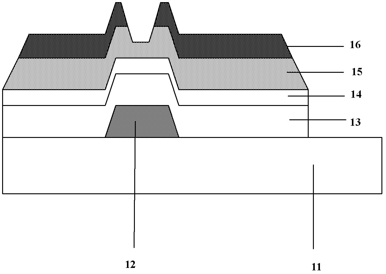
Embodiment 1
[0031] Such as figure 2 As shown, it is a flow chart of the preparation method of the gate insulating layer in Embodiment 1 of the present invention, including the following steps:
[0032] Step 101: Using PECVD technology, the substrate with the gate pattern is cleaned and sent to a vacuum chamber by a robot to deposit a first silicon nitride layer.
[0033] The substrate may be a glass substrate.
[0034] In this step 101, a radio frequency source with a radio frequency of 13.56 MHz is used to generate low temperature plasma, which is used as an energy source for gas reaction.
[0035] Under certain process conditions, the reaction gas silane (SiH 4 ), ammonia (NH 3 ), nitrogen (N 2 ), depositing the first silicon nitride layer. The certain process conditions refer to: the radio frequency power range is 8000W ~ 10000W, SiH 4 flow and NH 3 The flow ratio is between 0.2 and 0.4.
[0036] The deposition thickness of the first silicon nitride layer in this step 101 is ...
Embodiment 2
[0064] The second embodiment uses a specific example to illustrate the method in the first embodiment.
[0065] The method of the present embodiment 2 comprises the following steps:
[0066] Step 1: In this step, the first silicon nitride layer and the second silicon nitride layer can be deposited in the same manner as in step 101 and step 102 of the first embodiment.
[0067] Step 2: Deposit a nitrogen-doped amorphous silicon layer on the second silicon nitride layer by using the following deposition parameters.
[0068] The deposition parameters specifically include: RF power is 1500W, SiH 4 The flow rate is 2000sccm, NH 3 The flow rate is 100sccm, at this time SiH 4 flow and NH 3 The flow ratio was 20.
[0069] Terminate as soon as the second step starts N 2 access, start H 2 access, H 2 The flow rate is 10000 sccm.
[0070] The deposited nitrogen-doped amorphous silicon layer is
Embodiment 3
[0072] This embodiment provides a TFT and a preparation method thereof. The TFT preparation method includes the step of preparing a gate insulating layer by using the above-mentioned method for preparing a gate insulating layer; the TFT uses the above-mentioned gate insulating layer.
[0073] The TFT manufacturing method of this embodiment, except for the step of preparing the gate insulating layer by using the above-mentioned method for preparing the gate insulating layer, does not limit other process steps, that is, in addition to the method of forming the gate insulating layer, such as For the formation of other layers such as the gate electrode, the source-drain metal layer, and the pixel electrode, corresponding and achievable suitable methods can be used.
[0074] In addition to using the above-mentioned gate insulating layer, the TFT of this embodiment does not impose restrictions on other layers such as the gate, source-drain metal layer, and pixel electrode, that is, ...
PUM
 Abstract
Description
Claims
Application Information