Method for preparing silicon nano-pillar array based on nanosphere etching technology

A technology of nanosphere etching and silicon nanopillars, which is applied in microstructure technology, technology for producing decorative surface effects, decorative arts, etc., can solve complex processes, difficulties in large-area preparation, and the need to improve the stability of nanostructures, etc. problem, to achieve the effect of simple production process, good verticality, and improved specific capacity and specific power

Inactive Publication Date: 2012-08-15
XIAMEN UNIV
View PDF3 Cites 44 Cited by
  • Summary
  • Abstract
  • Description
  • Claims
  • Application Information

AI Technical Summary

Problems solved by technology

The stability of the currently prepared nanostructures needs to be improved, the process is relatively complicated, and it is relatively difficult to prepare large areas.

Method used


Image

  • Method for preparing silicon nano-pillar array based on nanosphere etching technology
  • Method for preparing silicon nano-pillar array based on nanosphere etching technology
  • Method for preparing silicon nano-pillar array based on nanosphere etching technology

Examples


Embodiment 1

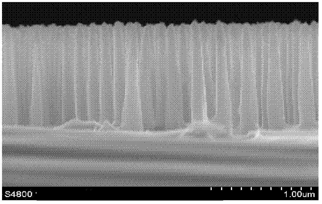
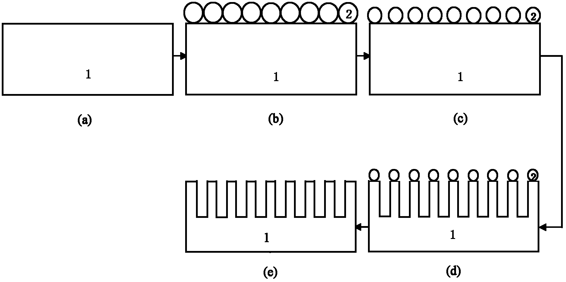
[0025] 1) First use standard cleaning on the silicon substrate, and then use the RIE system to activate the silicon wafer at a power of 60-80W for 3-10 minutes, which increases the hydrophilicity of the silicon wafer surface and is beneficial to obtain a large-area single-layer PS Nanospheres (Figure-1a).

[0026] In step 1), the size of the silicon wafer may be less than or equal to 100 mm, and the thickness may be 300-500 μm; the cleaning process may be:

[0027] (1) Sonicate the acetone solution for 3 to 5 minutes, and the absolute ethanol for 3 to 5 minutes, repeat twice before and after, then rinse with hot and cold deionized water;

[0028] (2) Use HF solution (HF:H 2 O) Soak for 30s and rinse with deionized water for 15 minutes;

[0029] (3) Use lotion I (NH 4 OH: H 2 O 2 : H 2 O), first heat the deionized water to 85℃ and pour NH 4 OH and H 2 O 2 , Put the chip into the beaker, cook for 15 minutes, and rinse with deionized water 6 to 7 times;

[0030] (4) Use diluted HF solutio...

Embodiment 2

[0044] Firstly, the standard cleaned silicon wafer (size: 50mm) is activated for 5 minutes in an RIE system with a power of 80W, and then a single-layer PS nanosphere (diameter 330nm) is self-assembled. The rotation speed is controlled at 500rpm and the spin coating time is 30s. High speed 2500rpm, spin coating time 40s. Subsequently, the above-mentioned Si wafer with a single-layer PS nanosphere as a mask was placed in an RIE system with a power of 80W for etching for 30s. The next step is to put the above-mentioned processed sample into the ICP system for etching treatment, and the etching gas SF 6 Flow rate 50sccm / min, time 7s, sidewall shielding gas C 4 F 8 Flow rate is 100sccm / min, time is 5s. Cycle 40. The ion source power is 1000W, the substrate bias power is 20W, the reaction chamber pressure is 6mT, and the reaction chamber temperature is 20°C. Finally, the etched sample was soaked in tetrahydrofuran for 10 hours, and then ultrasonically cleaned with acetone and alco...


PUM

PropertyMeasurementUnit
sizeaaaaaaaaaa
thicknessaaaaaaaaaa
diameteraaaaaaaaaa

Abstract

A method for preparing a silicon nano-pillar array based on nanosphere etching technology relates to a Si nano-structure. The method comprises the following steps of: after cleaning a silicon slice, performing activation treatment on the silicon slice by means of a reactive ion etching system, thereby obtaining a silicon slice surface with hydrophilicity; self-assembling single-layer polystyrene nanospheres on a silicon substrate by a spin coating method; regulating and controlling the diameters of the single-layer polystyrene nanospheres by means of the reactive ion etching system, thereby obtaining the single-layer polystyrene nanospheres different in diameter; taking the single-layer polystyrene nanospheres as masks, performing etching by means of the masks and by inductively coupled plasma etching technology, and performing etching and sidewall protection by alternately using SF6 and C4F8; and removing the masks and by-products produced in the etching process by using an organic reagent, thus finally obtaining the silicon nano-pillar array.

Description

Technical field [0001] The invention relates to a Si nano structure, in particular to a method for preparing a silicon nano column array based on nano ball etching technology. Background technique [0002] At present, there are many methods for the preparation of Si nanocolumn / wire structures, such as the use of metals (such as Au) to catalyze the chemical vapor deposition (Chemical Vapor Deposition, referred to as CVD) bottom-up synthesis of Si nanowires (Yi Cui et al. , Nano letters 31, 35, 2007), metal-catalyzed chemical wet etching (Jr-Hau He et al, Langmuir 12855, 12858, 2010), dry etching (Shigehito Deki et al, Microelectronic Engineering 355, 364, 2008) Wait for the top-down approach. Compared with chemical synthesis and wet etching methods, the Si nanostructure prepared by dry etching technology has the characteristics of good verticality, relatively high depth and width, orderly arrangement, and relatively mature technology. As far as dry etching is concerned, ICP or R...

Claims


Application Information

Patent Timeline
Patent Type & Authority Applications(China)
IPC IPC(8): B81C1/00
Inventor 李静岳闯尹君臧雅姝何绪吴孙桃
Owner XIAMEN UNIV
Why Eureka
Try Eureka