Micro-mechanical magnetic field sensor and preparation method thereof
A magnetic field sensor and micro-mechanical technology, applied in the field of magnetic field sensors, can solve the problems of poor anti-interference, complex structure, high power consumption, etc., and achieve the effects of increased strength, reduced complexity, and reduced power consumption
- Summary
- Abstract
- Description
- Claims
- Application Information
AI Technical Summary
Problems solved by technology
Method used
Image
Examples
Embodiment 1
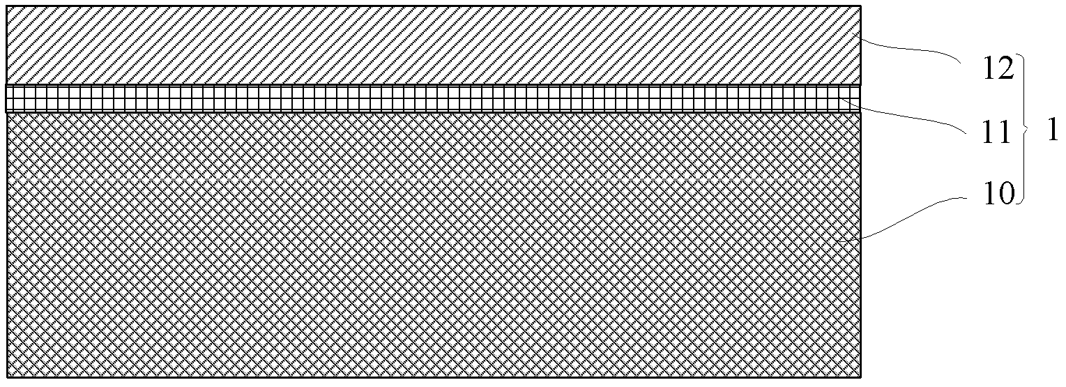
[0077] Such as Figure 1a to Figure 1i Shown, the present invention provides a kind of preparation method of micromechanical magnetic field sensor, comprises the following steps:
[0078] Step 1: If Figure 1a As shown, an SOI substrate 1 is provided, including substrate silicon 10 , buried oxide layer 11 , and top layer silicon 12 .
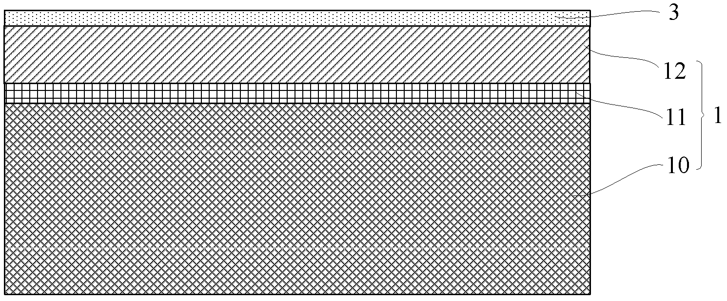
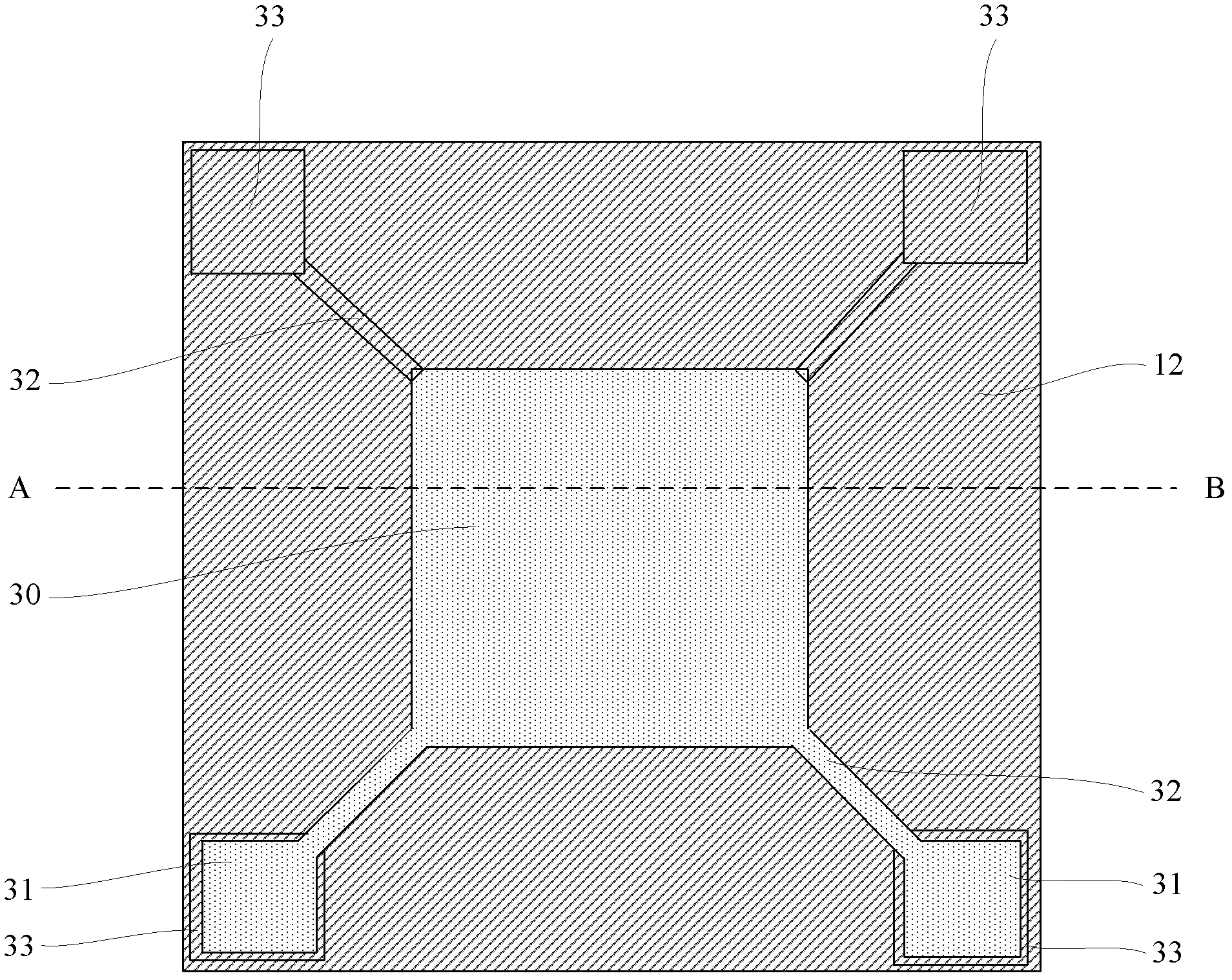
[0079] Step 2: If Figure 1b to Figure 1d As shown, a layer of electrical insulating dielectric layer 3 is deposited by thermal growth or LPCVD on the top layer of silicon of the SOI substrate 1, and the electrical insulating dielectric layer 3 is patterned and etched to retain the corresponding resonator Area 30, the pre-prepared test pad area 31, the pre-prepared support beam area 32, and the pre-prepared electrical insulating medium layer 3 of the anchor point area 33, wherein Figure 1c For the process plan formed in this step, Figure 1d for along Figure 1c A cross-sectional view of the AB direction.
[0080] Specifically, the number...
Embodiment 2
[0090] Such as Figure 2a As shown, an SOI substrate is provided, and a cavity 2 is pre-opened between the top layer silicon 12 and the buried oxide layer 11 of the SOI substrate 1. The formation process of the cavity 2 is well known to those skilled in the art. Conventional process: first, patterned photolithography is performed on the substrate silicon 10, and then a groove (not shown) deep to the buried oxide layer is etched according to the photolithographic pattern. The groove is a square groove, a circular groove The groove, or the annular groove, is preferably a square groove in this embodiment. Then thermally grow a layer of silicon oxide on the bottom of the groove and the peripheral sidewall as the buried oxide layer 11, and finally bond a layer of silicon on the side with the groove as the top layer of silicon 12, the top layer of silicon 12 and The cavity between the buried oxide layers 11 is the cavity 2 .
[0091] The main difference between the process of prep...
Embodiment 3
[0093] As shown in the figure, the present invention provides a method for preparing a micromechanical magnetic field sensor, comprising the following steps:
[0094] Step 1: If Figure 3a As shown, an SOI substrate 1 is provided, including substrate silicon 10 , buried oxide layer 11 , and top layer silicon 12 .
[0095] Step 2: If Figure 3b to Figure 3d As shown, a layer of electrical insulating dielectric layer 3 is thermally grown or LPCVD deposited on the top layer of silicon of the SOI substrate 1, and the electrical insulating dielectric layer 3 is patterned and etched to retain the corresponding pre-prepared The resonator area 30, the pre-prepared test pad area 31, the pre-prepared support beam area 32, and the pre-prepared electrical insulating medium layer 3 of the anchor point area 33, wherein Figure 3c It is the process structure plan formed in this step, Figure 3d for along Figure 3c A cross-sectional view of the AB side.
[0096] Specifically, the number...
PUM
 Abstract
Description
Claims
Application Information


