
Nano-structure layer for gallium-nitride-based (GaN-based) light emitting diode (LED) epitaxial slice and preparation method thereof

An LED epitaxial wafer and nanostructure technology, which is applied in electrical components, circuits, semiconductor devices, etc., can solve the problems of large non-radiative loss, easy oxidation of metal Ag, reduce surface plasmon coupling output, etc., to improve luminous efficiency. , the effect of preventing oxidation and reducing production costs

Inactive Publication Date: 2012-09-19
INST OF PHYSICS - CHINESE ACAD OF SCI
View PDF1 Cites 15 Cited by
  • Summary
  • Abstract
  • Description
  • Claims
  • Application Information

AI Technical Summary

Problems solved by technology

[0004] At present, the method of using surface plasmons to enhance the luminous efficiency of LEDs is mainly to deposit metal thin films (such as Ag films) on the surface of LED epitaxial wafers (such as InGaN / GaN quantum well epitaxial wafers, whose luminous wavelength is 400-560nm) using semiconductor technology. , but the films deposited by this method are all polycrystalline structures, and the collective oscillation of electrons after surface plasmon excitation occurs between many crystal domains, resulting in a large non-radiative loss, which weakens the surface plasmon enhancement. glowing effect
Another method is to use micro-nano processing techniques such as electron beam exposure to obtain metal nanoparticles, but the formed metal Ag is very easy to oxidize, and the oxidation will form a silver oxide layer without surface plasmon effect, so it will reduce the surface plasmon excitation. Coupling output of element pair energy

Method used


Image

  • Nano-structure layer for gallium-nitride-based (GaN-based) light emitting diode (LED) epitaxial slice and preparation method thereof
  • Nano-structure layer for gallium-nitride-based (GaN-based) light emitting diode (LED) epitaxial slice and preparation method thereof
  • Nano-structure layer for gallium-nitride-based (GaN-based) light emitting diode (LED) epitaxial slice and preparation method thereof

Examples


Embodiment Construction

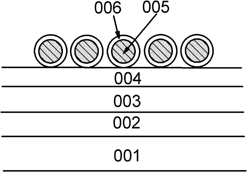
[0028] Below to figure 1 The blue-light GaN-based LED epitaxial wafer with an emission wavelength of 480 nm is taken as an example to illustrate the present invention in detail.

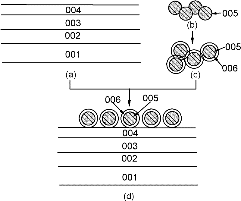
[0029] Such as figure 1 As shown, the LED epitaxial wafer includes a substrate 001, which can be a common LED substrate material such as sapphire. Located on the substrate 001 is a buffer layer 002, such as a GaN layer with certain doping. InGaN / GaN quantum well structure 003 (InGaN is the well layer, GaN is the barrier layer) is located on the buffer layer 002, and the light emission wavelength is around 480nm, which is the active part of the epitaxial wafer. On the InGaN / GaN quantum well layer is a GaN isolation layer 004 with a thickness of about 50nm to reduce the annihilation of the light field. The LED epitaxial wafer may also include a layer (or film) containing a plurality of Ag nanoparticles 005 (with a single crystal structure), wherein the surface of each Ag nanoparticle 005 is coated w...


PUM

PropertyMeasurementUnit
radiusaaaaaaaaaa
thicknessaaaaaaaaaa
emission peakaaaaaaaaaa

Abstract

The invention provides a nano-structure layer for a gallium-nitride-based (GaN-based) light emitting diode (LED) epitaxial slice. The nano-structure layer comprises a silver (Ag) film which is located on the surface of the epitaxial slice and has an energy coupling with the epitaxial slice, and the Ag film is composed of a plurality of spherical Ag nano-particles. The nano-structure layer is characterized in that a sulfur dioxide (SiO2) film is coated on the outer surfaces of the Ag nano-particles. The nano-particles which are in metal-medium nuclear shell structures are compounded by a chemical method, nano-particles in metal-medium nuclear shell structures are self-assembled on the surface of an indium gallium nitride (IN GaN) / GaN LED epitaxial slice, under the condition that the requirement of a surface plasmon phase matching is met, the energy is transferred to be a surface plasmon mode by a resonance coupling of a local surface plasmon and a quantum well to form effective radiation, the output of the light is increased, and the LED external quantum efficiency is improved.

Description

technical field [0001] The invention relates to a semiconductor optoelectronic device, in particular to a nanostructure layer for a GaN-based LED epitaxial wafer and a preparation method thereof. Background technique [0002] In the situation of increasingly tight energy sources, using LEDs as light sources is one of the main measures to save energy. However, at present, the light output efficiency and cost of LEDs are the main bottlenecks restricting applications such as LED white light lighting. Therefore, improving the luminous efficiency of LEDs and developing a new generation of high-brightness LEDs are the primary conditions for the widespread application of LEDs. For this reason, countries around the world have invested considerable funds and manpower in research and development. Japan took the lead in carrying out the "21st Century Lighting Plan", the US Department of Energy formulated the "National Research Project on Semiconductor Lighting", and my country launched...

Claims


Application Information

Patent Timeline
Patent Type & Authority Applications(China)
IPC IPC(8): H01L33/00B22F9/24B22F1/02
Inventor 李敬徐红星
Owner INST OF PHYSICS - CHINESE ACAD OF SCI
Learn More