White light electroluminescent device

An electroluminescent device and luminescent technology, which is applied in the direction of electric solid-state devices, luminescent materials, electrical components, etc., can solve problems such as poor life and stability of blue light materials, restrictions on blue light emission, and rising device temperature, so as to improve Effect of hole transport ability and electron transport ability, improvement of luminous efficiency, and suppression of concentration quenching

Inactive Publication Date: 2012-10-17
OCEANS KING LIGHTING SCI&TECH CO LTD +1
View PDF5 Cites 5 Cited by
  • Summary
  • Abstract
  • Description
  • Claims
  • Application Information

AI Technical Summary

Problems solved by technology

[0004] Luminescent materials are the most important factor affecting luminous efficiency. Luminescent materials can be divided into fluorescent materials (ie, blue light materials) and phosphorescent materials (ie, red light phosphorescent materials and / or green light phosphorescent materials). Fluorescent materials are blocked due to triplet transitions. Therefore, it can only emit light through the radiation inactivation of the singlet state, and the ratio of the triplet excitons to the singlet excitons is about 3:1; and since only 25wt% of the excitons in the fluorescent material can be effectively used, the remaining 75wt % are all through non-radiative attenuation, the energy is released in the form of heat, which increases the temperature of the device, thereby reducing the life of the device, while the phosphorescent material is due to the strong spin coupling effect of the metal atom itself, so the original impossible three-line Therefore, the luminous efficiency is greatly improved. At present, the luminous efficiency of green phosphorescent materials and red phosphorescent materials is relatively good, and the material stability is high, while the life and stability of blue phosphorescent materials are not very good, which restricts blue light glow

Method used


Image

  • White light electroluminescent device
  • White light electroluminescent device
  • White light electroluminescent device

Examples


Embodiment 1

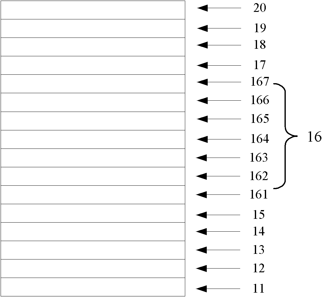
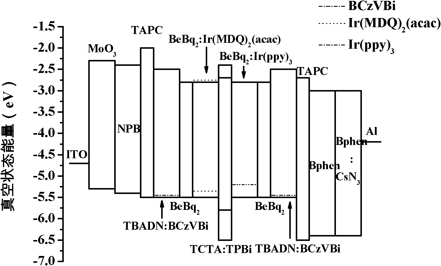
[0048] A white photoluminescent device, its layered structure is: glass / ITO / MoO 3 / NPB / TAPC / TBADN:BCzVBi / BeBq 2 / BeBq 2 :Ir(MDQ) 2 (acac) / TCTA:TPBi / BeBq 2 :Ir(ppy) 3 / BeBq 2 / TBADN:BCzVBi / TPBi / Bphen / Bphen:CsN 3 / Al.

[0049] First, photolithographically process the ITO glass, cut it into the required light-emitting area, and then use detergent, deionized water, acetone, ethanol, and isopropanol to ultrasonically clean the glass surface for 15 minutes to remove organic pollutants on the glass surface. It is subjected to oxygen plasma treatment, the treatment time is 5-15min, and the power is 50W; then each organic functional layer is sequentially vapor-deposited on the ITO conductive layer to obtain a white light electroluminescent device; wherein,

[0050] The material of the hole injection layer is MoO 3 , with a thickness of 5nm;

[0051] The material of the hole transport layer is NPB with a thickness of 10nm;

[0052] The material of the electron blocking layer i...

Embodiment 2

[0068] A white electroluminescent device, its layered structure is: glass / ITO / WO 3 / TPD / TAPC / TPD:TBPe / BeqQ 2 / BeqQ 2 :Ir(MDQ) 2 (acac) / TBADN:PBD / BeqQ 2 :Ir(ppy) 3 / BeqQ 2 / TCTA:perylene / AIq 3 / BND / Cs 2 CO 3 / Ag.

[0069] First, photolithographically process the ITO glass, cut it into the required light-emitting area, and then use detergent, deionized water, acetone, ethanol, and isopropanol to ultrasonically clean the glass surface for 15 minutes to remove organic pollutants on the glass surface. It is subjected to oxygen plasma treatment, the treatment time is 10min, and the power is 50W; then each organic functional layer is sequentially vapor-deposited on the ITO conductive layer to obtain a white light electroluminescence device; wherein,

[0070] The material of the hole injection layer is WO 3 , with a thickness of 10nm;

[0071] The material of the hole transport layer is TPD with a thickness of 5nm;

[0072] The material of the electron blocking layer is TA...

Embodiment 3

[0085] A white electroluminescent device, its layered structure is: glass / ITO / VO x / TCTA / NPB / TCTA:DPAVBi / BeqQ 2 / BeqQ 2 :Ir(piq) 2 (acac) / CBP:Alq 3 / BeqQ 2 :Ir(ppy) 2 (acac)) / BeMQ 2 / TDAPB:DPAVB / BND / TAZ / CsN 3 / Ag-Mg.

[0086] First, photolithographically process the ITO glass, cut it into the required light-emitting area, and then use detergent, deionized water, acetone, ethanol, and isopropanol to ultrasonically clean the glass surface for 15 minutes to remove organic pollutants on the glass surface. It is subjected to oxygen plasma treatment, the treatment time is 15min, and the power is 50W; then each organic functional layer is sequentially vapor-deposited on the ITO conductive layer to obtain a white light electroluminescent device; wherein,

[0087] The material of the hole injection layer is VO x , with a thickness of 40nm;

[0088] The material of the hole transport layer is TCTA with a thickness of 80nm;

[0089] The electron blocking layer is made of NPB w...


PUM

PropertyMeasurementUnit
Thicknessaaaaaaaaaa
Thicknessaaaaaaaaaa
Thicknessaaaaaaaaaa

Abstract

The invention pertains to the field of optoelectronic devices, and discloses a white light electroluminescent device. The device has a layered structure. The layered structure sequentially includes: a substrate / an electrically conductive layer / a hole injection layer / a hole transporting layer / an electron barrier layer / a first blue light emitting layer / a first barrier layer / a red light emitting phosphor layer / a spacer layer / a green light emitting phosphor layer / a second barrier layer / a second blue light emitting layer / a hole barrier layer / an electron transporting layer / an electron injection layer / a cathode layer. The materials of the first and second blue light emitting layers both are a hole transporting material doped with a blue light emitting material, and the materials of the red light emitting phosphor layer and the green light emitting phosphor layer are a beryllium complex material doped with a red light emitting phosphor material and a beryllium complex material doped with a green light emitting phosphor material respectively. According to the white light electroluminescent device of the invention, the first and second barrier layers are respectively arranged between the first blue light emitting layer and the red light emitting phosphor layer, and between the second blue light emitting layer and the green light emitting phosphor layer, so triplet excitons of the blue light emitting material can be diffused into the red light emitting phosphor layer and the green light emitting phosphor layer to undergo radiative transition so as to emit light, so that light emitting efficiency of the device is further improved.

Description

technical field [0001] The invention relates to the field of optoelectronic devices, in particular to a white light electroluminescence device. Background technique [0002] In 1987, C.W.Tang and Van Slyke of Eastman Kodak Company in the United States reported a breakthrough in the research of organic electroluminescence. A high-brightness, high-efficiency double-layer organic electroluminescent device (OLED) was prepared by using ultra-thin film technology. In this double-layer structure device, the brightness reaches 1000cd / m at 10V 2 , its luminous efficiency is 1.51lm / W, and its lifespan is more than 100 hours. [0003] The principle of OLED light emission is based on the action of an external electric field, electrons are injected from the cathode to the lowest unoccupied molecular orbital (LUMO) of organic matter, and holes are injected from the anode to the highest occupied orbital (HOMO) of organic matter. Electrons and holes meet, recombine, and form excitons in ...

Claims


Application Information

Patent Timeline
IPC IPC(8): H01L51/50H01L51/52H01L51/54C09K11/06
CPCY02B20/181Y02B20/00
Inventor 周明杰王平黄辉陈吉星
Owner OCEANS KING LIGHTING SCI&TECH CO LTD
Why Eureka
Try Eureka