SiGe based strain BiCMOS (Bipolar Complementary Metal-Oxide-Semiconductor Transistor) integrated device and preparation method thereof

A technology for MOS devices and integrated devices, which is applied in semiconductor/solid-state device manufacturing, electrical solid-state devices, semiconductor devices, etc., and can solve problems such as the inability to meet low power consumption, the inability to meet the requirements of lithography technology, and the impact of device performance.

Inactive Publication Date: 2012-10-24
XIDIAN UNIV
View PDF3 Cites 0 Cited by
  • Summary
  • Abstract
  • Description
  • Claims
  • Application Information

AI Technical Summary

Problems solved by technology

For example, when the feature size is less than 100nm, due to problems such as tunneling leakage current and reliability, the traditional gate dielectric material SiO 2 Unable to meet the requirements of low power consumption; the short channel effect and narrow channel effect of nanometer devices are becoming more and more obvious, which seriously affects the device performance; traditional lithography technology cannot meet the shrinking lithography precision
Therefore, traditional Si-based process devices are increasingly difficult to meet the needs of design

Method used


Image

  • SiGe based strain BiCMOS (Bipolar Complementary Metal-Oxide-Semiconductor Transistor) integrated device and preparation method thereof

Examples


Embodiment 1

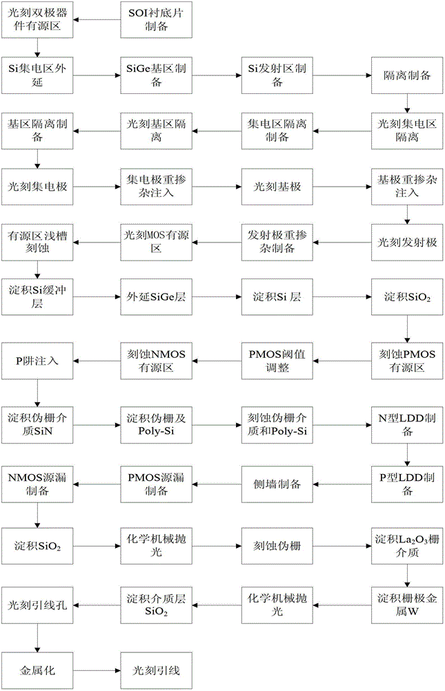
[0116] Embodiment 1: To prepare a SiGe-based strained BiCMOS integrated device and circuit with a channel length of 22nm, the specific steps are as follows:

[0117] Step 1, SOI substrate material preparation.

[0118] (1a) Select the N-type doping concentration as 1×10 15 cm -3 The Si sheet is oxidized on its surface, and the thickness of the oxide layer is 1 μm, which is used as the base material of the upper layer, and hydrogen is injected into the base material;

[0119] (1b) Select the N-type doping concentration as 1×10 15 cm -3 The Si sheet is oxidized on its surface, and the thickness of the oxide layer is 1 μm, which is used as the base material of the lower layer;

[0120] (1c) Using a chemical mechanical polishing (CMP) process to polish the surface of the lower layer and the upper layer of substrate material after hydrogen injection;

[0121] (1d) Put the oxide layer on the surface of the polished lower layer and the upper layer of the base material relatively...

Embodiment 2

[0183] Embodiment 2: To prepare a SiGe-based strained BiCMOS integrated device and circuit with a channel length of 130nm, the specific steps are as follows:

[0184] Step 1, SOI substrate material preparation.

[0185] (1a) Select the N-type doping concentration as 3×10 15 cm -3 The Si sheet is oxidized on its surface, and the thickness of the oxide layer is 0.7 μm, which is used as the base material of the upper layer, and hydrogen is injected into the base material;

[0186] (1b) Select the N-type doping concentration as 3×10 15 cm -3 The Si sheet is oxidized on its surface, and the thickness of the oxide layer is 0.7 μm, which is used as the base material of the lower layer;

[0187] (1c) Using a chemical mechanical polishing (CMP) process to polish the surface of the lower layer and the upper layer of substrate material after hydrogen injection;

[0188] (1d) Put the oxide layer on the surface of the polished lower layer and the upper layer of the base material relat...

Embodiment 3

[0250] Embodiment 3: The preparation of SiGe-based strained BiCMOS integrated devices and circuits with a channel length of 350nm, the specific steps are as follows:

[0251] Step 1, SOI substrate material preparation.

[0252] (1a) Select the N-type doping concentration as 5×10 15 cm -3 The Si sheet is oxidized on its surface, and the thickness of the oxide layer is 0.5 μm, which is used as the base material of the upper layer, and hydrogen is injected into the base material;

[0253] (1b) Select the N-type doping concentration as 5×10 15 cm -3 The Si sheet is oxidized on its surface, and the thickness of the oxide layer is 0.5 μm, which is used as the base material of the lower layer;

[0254] (1c) Using a chemical mechanical polishing (CMP) process to polish the surface of the substrate material of the lower layer and the upper layer of the active layer after injecting hydrogen, respectively;

[0255] (1d) Put the oxide layer on the surface of the polished lower layer ...


PUM

PropertyMeasurementUnit
Thicknessaaaaaaaaaa
Thicknessaaaaaaaaaa
Thicknessaaaaaaaaaa

Abstract

The invention discloses a SiGe based strain BiCMOS (Bipolar Complementary Metal-Oxide-Semiconductor Transistor) integrated device and a preparation method thereof. The preparation method comprises the steps of: first, preparing an SOI (Silicon On Insulator) substrate, continuously growing an N-Si layer, a P-SiGe layer and an N-Si layer to prepare a deep trench isolation region; respectively carrying out photo-etching on a shallow trench isolation region of a collector region and a shallow trench isolation region of a base region; carrying out ion injection to form a collecting electrode contact region, a base electrode contact region and an emitting electrode contact region, and finally forming a SiGe HBT (Heterojunction Bipolar Transistor) device; then carrying out photo-etching on an active region of an MOS (Metal Oxide Semiconductor), continuously growing a Si buffer layer, a strain SiGe layer and an intrinsic Si layer in the region to respectively form active regions of an NMOS (N-channel Metal Oxide Semiconductor) and a PMOS (P-channel Metal Oxide Semiconductor); depositing SiO2 and polycrystalline silicon in the active regions of the NMOS and the PMOS, preparing a fake grid electrode which is 22-350nm long; forming a light dope source drain electrode (LDD) and a source drain electrode of NMOS and PMOS devices by a self-aligning process, then removing the fake grid electrode, preparing grid medium lanthanum oxide (La2O3) and metal wolfram (W) to form a grid electrode; and finally metalizing, and carrying out photo-etching on a lead to form the BiCMOS integrated device and a circuit. According to the SiGe based strain BiCMOS integrated device and the preparation method of the SiGe based strain BiCMOS integrated device provided by the invention, influence of the hot carrier on the performance of the device is inhibited effectively and the reliability of the device is improved due to the adoption of the structure of the light dope source drain electrode.

Description

technical field [0001] The invention belongs to the technical field of semiconductor integrated circuits, in particular to a SiGe-based strained BiCMOS integrated device and a preparation method. Background technique [0002] Semiconductor integrated circuit technology is the core technology of high-tech and information industries, and has become an important symbol to measure a country's scientific and technological level, comprehensive national strength and national defense strength, while microelectronic technology represented by integrated circuits is the key to semiconductor technology. The semiconductor industry is the basic industry of the country. The reason why it develops so fast is not only the huge contribution of technology itself to economic development, but also its wide applicability. [0003] Gordon Moore, one of the founders of Intel, proposed "Moore's Law" in 1965, which states that the number of transistors on an integrated circuit chip doubles about ever...

Claims


Application Information

Patent Timeline
IPC IPC(8): H01L27/12H01L21/84
Inventor 胡辉勇张鹤鸣宋建军周春宇舒斌宣荣喜戴显英郝跃
Owner XIDIAN UNIV
Why Eureka
Try Eureka