Light emitting diode by taking graphene film as current carrier injection layer

A graphene film, light-emitting diode technology, applied in electrical components, circuits, semiconductor devices, etc., can solve the problems of uneven current distribution, large effective hole mass, increased production cost and cycle, etc.

Inactive Publication Date: 2012-10-24
INST OF SEMICONDUCTORS - CHINESE ACAD OF SCI
View PDF2 Cites 7 Cited by
  • Summary
  • Abstract
  • Description
  • Claims
  • Application Information

AI Technical Summary

Problems solved by technology

On the other hand, due to the difficulty of P-type doping and the large effective mass of holes, the asymmetry of electron-hole injection is the main problem in light-emitting diodes.
At the same time, in order to

Method used


Image

  • Light emitting diode by taking graphene film as current carrier injection layer
  • Light emitting diode by taking graphene film as current carrier injection layer
  • Light emitting diode by taking graphene film as current carrier injection layer

Examples


Embodiment

[0034] see Figure 1 to Figure 4 Shown, a kind of graphene film of the present invention is used as the light-emitting diode of carrier injection layer, comprises the following steps:

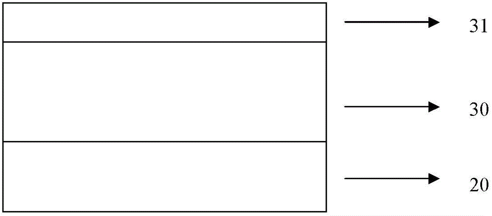
[0035] 1. On the sapphire substrate 20, epitaxially grow a 0.1 μm thick GaN buffer layer, a 2 μm thick non-doped GaN, a 2 μm thick heavily doped Si n-type GaN electron injection layer 30, and 8 pairs of quantum wells GaN / InGaN to emit light Layer 31 (total thickness 0.15 μm). ;

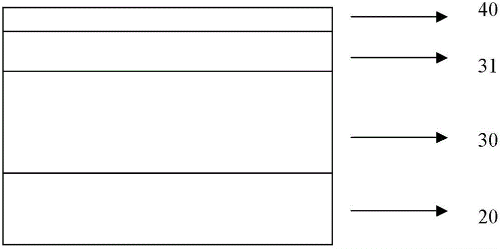
[0036] 2. Paste the prepared graphene film 40 on the surface of the epitaxial structure, place it in concentrated nitric acid vapor for 1 minute, and then vacuum anneal for 3 minutes;

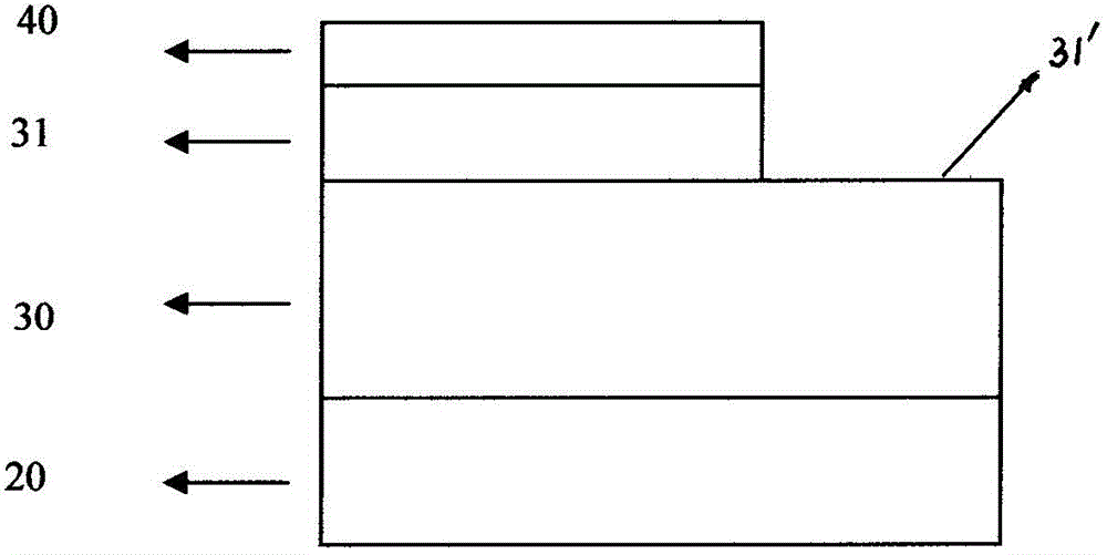
[0037] 3. Selectively etch the epitaxial structure by photolithography, inductively coupled plasma etching and other processes to expose the N-type GaN electron injection layer to form a mesa 31';

[0038] 4. Prepare the aluminum (Al) / titanium (Ti) / gold (Au) (400 / 50 / 400nm) N-type metal electrode 50 on the table 31' through photolitho...


PUM


Abstract

The invention discloses a light emitting diode by taking a graphene film as a current carrier injection layer, which comprises a substrate, a current carrier injection layer, a luminescent layer, a graphene film, a lower metal electrode and an upper metal electrode, wherein the current carrier injection layer is manufactured on the substrate; the luminescent layer is manufactured on one side of the upper surface of the current carrier injection layer, and the width of the luminescent layer is smaller than the width of the current carrier injection layer to enable the current carrier injection layer to form a table top; the graphene film is manufactured on the luminescent layer; the lower metal electrode is manufactured on the table top of the current carrier injection layer; and the upper metal electrode is manufactured on the graphene film. According to the light emitting diode disclosed by the invention, a method that the graphene film is used as the current carrier injection layer is adopted, the hole injection is improved, the thickness of an electronic injection layer is reduced, and the cost is lowered.

Description

technical field [0001] The invention belongs to the technical field of semiconductors, in particular to a gallium nitride-based light-emitting diode using a graphene film as a carrier injection layer. Background technique [0002] Graphene is a carbon atom with sp 2 The planar film with hexagonal honeycomb lattice composed of hybrid orbitals has high transmittance (97.7%); high thermal conductivity (5300W / m K), high electron mobility (15000 cm 2 / V·s), the low resistivity is only about (10 -6 Ω·cm). Because of its extremely low resistivity and high electron mobility, it is expected to be used to develop a new generation of electronic components or transistors that are thinner and conduct electricity faster. It has been used in the manufacture of transparent conductive layers, touch screens, light panels and solar cells. On the other hand, due to the difficulty of P-type doping and the large effective mass of holes, the asymmetry of electron-hole injection is the main pro...

Claims


Application Information

Patent Timeline
IPC IPC(8): H01L33/14H01L33/04
Inventor 马骏汪炼成张逸韵伊晓燕王国宏
Owner INST OF SEMICONDUCTORS - CHINESE ACAD OF SCI
Why Eureka
Try Eureka