Organic light emitting diode

A light-emitting diode, organic technology, applied in the field of electronics, can solve the problems of large emission spectrum changes, weak fluorescent blue light emission, spectral instability, etc., to achieve the effects of improving luminous efficiency, good spectral stability, and improved stability

Active Publication Date: 2012-10-24
CHANGCHUN INST OF APPLIED CHEMISTRY - CHINESE ACAD OF SCI
View PDF4 Cites 12 Cited by
  • Summary
  • Abstract
  • Description
  • Claims
  • Application Information

AI Technical Summary

Problems solved by technology

However, due to the weak emission of fluorescent blue light, the obtained spectrum is yellowish, and its emission spectrum changes greatly with the increase of driving voltage, showing serious spectral instability.

Method used


Image

  • Organic light emitting diode
  • Organic light emitting diode
  • Organic light emitting diode

Examples


preparation example Construction

[0064] The preparation method of the organic light-emitting diode of the present invention is specifically prepared according to the following method:

[0065] First photoetch the ITO layer 2 on the ITO glass into a thin strip electrode, then clean it, dry it with nitrogen, bake it in a vacuum oven at 120°C for 0.5~1h, treat it with oxygen plasma for 1~5min, and then transfer it In the vacuum coating system, wait until the vacuum degree reaches 1~5×10 -4 At Pa, on the ITO layer 2, a hole interface layer 3, a hole transport layer 4, an electron / exciton blocking layer 5, a red phosphorescent dye-doped light-emitting layer 6, a spacer layer 7, and a green phosphorescent dye doped Miscellaneous light-emitting layer 8, electron transport / hole blocking layer 9, electron interface layer 10 and cathode 11, where the two electrodes cross each other to form the light-emitting area of ​​the device, and the area of ​​the light-emitting area is 16mm 2 , the hole interface layer 3 has a thic...

Embodiment 1

[0069] First, the ITO anode 2 on the glass substrate 1 is photolithographically formed into an electrode with a width of 4 mm and a length of 30 mm, then cleaned, blown dry with nitrogen, placed the glass in a vacuum oven and baked at 120°C for 30 minutes, then sprayed with oxygen plasma After processing for 2 minutes, put the glass into the vacuum coating system. When the vacuum degree of the vacuum coating system reaches 1~5×10 -4 Pa, sequentially vapor-deposit MoO on the ITO anode 2 3 Hole interface layer 3, NPB hole transport layer 4, TAPC electron / exciton blocking layer 5, red phosphorescent dye Ir (MDQ) 2(acac) Emitting layer 6 doped with hole transport material TCTA, hole transport material TCTA and electron transport material Be(PP) 2 Mixed spacer layer 7, green phosphorescent dye (ppy) 2 Ir (acac) Doped electron transport material Be(PP) 2 The light-emitting layer 8, Be (PP) 2 The electron transport / hole blocking layer 9, the electron interface layer 10 of LiF a...

Embodiment 2

[0072] The preparation method is the same as that of Example 1, the difference is: (ppy) 2 Ir (acac) In Be (PP) 2 The doping concentration in is controlled at 0.3wt%.

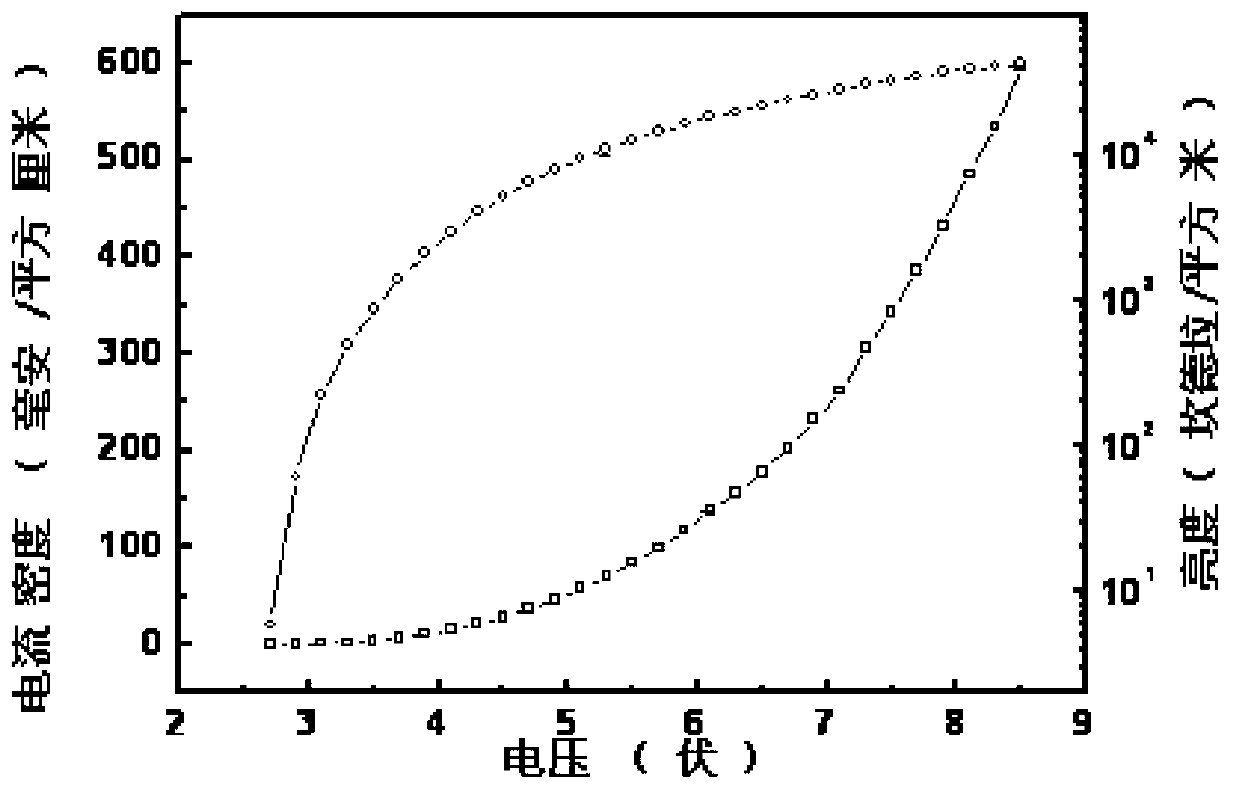
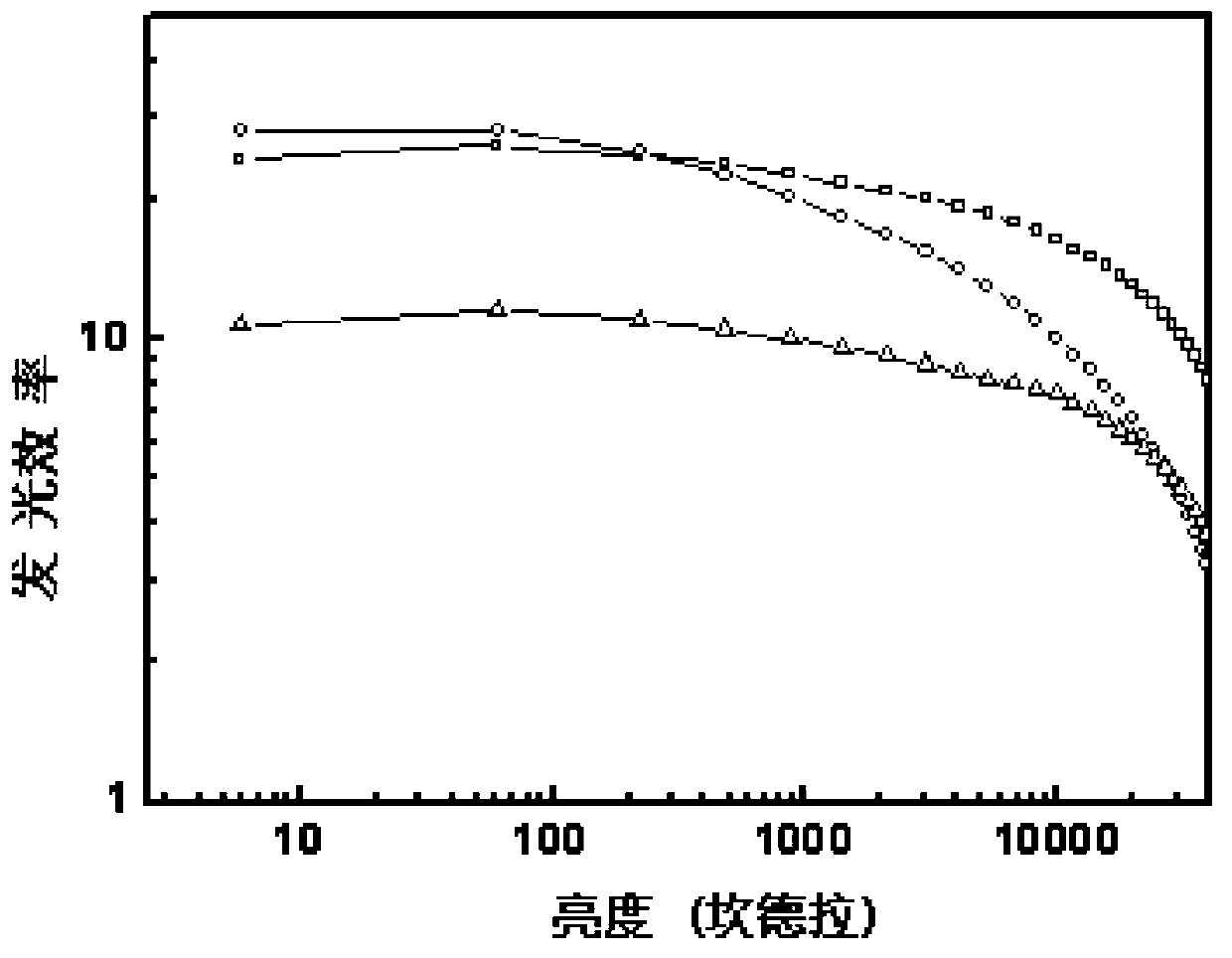
[0073] Figure 5 The current density-brightness-voltage characteristic curve of the fluorescent / phosphorescent hybrid white light organic light-emitting diode prepared for Example 2, the ○ curve in the figure is the brightness-voltage curve of the organic light-emitting diode, and the □ curve is the current density-voltage of the organic light-emitting diode curve, by Figure 5 It can be seen that the lighting voltage of the device is 2.6 volts, and the maximum brightness of the device exceeds 50000cd / m 2 , the brightness at 3.3V voltage is 1000cd / m 2 . Figure 6 is the brightness-power efficiency-current efficiency-quantum efficiency characteristic curve of the device, the □ curve in the figure is the current efficiency curve of the diode, ○ is the power efficiency curve of the diode, and the △ curve is ...


PUM

PropertyMeasurementUnit
band gapaaaaaaaaaa
thicknessaaaaaaaaaa
thicknessaaaaaaaaaa

Abstract

The invention provides an organic light emitting diode, which comprises a substrate, a first electrode, a second electrode and an organic light emitting unit, wherein the first electrode is arranged on the substrate; the second electrode is arranged on the first electrode; the organic light emitting unit is arranged between the first electrode and the second electrode; the organic light emitting unit comprises a red-light phosphorescent dye doped hole-transmission material light emitting layer, a spacing layer and a green-light phosphorescent dye doped blue-light electronic transmission light emitting layer, which are sequentially laminated; and the spacing layer consists of a hole transmission material and an electronic transmission material. The light emitting unit is provided with the red-light phosphorescent dye doped light emitting layer, the spacing layer and the green-light phosphorescent dye doped light emitting layer, and the spacing layer contains the electronic transmission material and the hole transmission material, so that a compounded area of the hole and electron is enlarged, exciton can be adequately utilized, and the organic light emitting diode has high efficiency, high stability and high color rendering index.

Description

technical field [0001] The invention relates to the field of electronic technology, in particular to an organic light emitting diode. Background technique [0002] Organic light-emitting diodes have many advantages such as full solid state, active light emission, high contrast, fast response, wide viewing angle, vivid color, high definition, ultra-thin and easy flexible display, and are emerging display technologies in the information field. After LCD It is expected to become the fastest-growing new flat-panel display technology in the next 20 years, and has been widely used in small and medium-sized color displays such as mobile phones, personal data processors, and car dashboards. [0003] Organic light-emitting diodes can achieve different light-emitting colors such as red, green, blue, or white light according to different light-emitting layers, especially the research on white light-emitting organic light-emitting diodes with a wide spectrum has attracted more and more ...

Claims


Application Information

Patent Timeline
Patent Type & Authority Applications(China)
IPC IPC(8): H01L51/52H01L51/54C09K11/06
Inventor 马东阁赵方超陈江山张智强代岩峰刘一鹏王艳平孙宁
Owner CHANGCHUN INST OF APPLIED CHEMISTRY - CHINESE ACAD OF SCI
Why Eureka
Try Eureka