Epitaxial wafer for 980nm F-P cavity strained quantum well laser with narrow line width and preparation method thereof

A 980nmf-p, quantum well technology, applied in the field of semiconductor lasers, to achieve the effect of low linewidth factor, improved quality, and reduced linewidth

Active Publication Date: 2012-11-14
YANGZHOU CHANGELIGHT
View PDF4 Cites 5 Cited by
  • Summary
  • Abstract
  • Description
  • Claims
  • Application Information

AI Technical Summary

Problems solved by technology

[0005] In order to solve the problems existing in the line width of the existing 980nm F-P cavity strained quantum well laser, the present invention provides an epitaxial wafer of a low line width 980nm F-P cavity strained quantum well laser

Method used


Image

  • Epitaxial wafer for 980nm F-P cavity strained quantum well laser with narrow line width and preparation method thereof
  • Epitaxial wafer for 980nm F-P cavity strained quantum well laser with narrow line width and preparation method thereof
  • Epitaxial wafer for 980nm F-P cavity strained quantum well laser with narrow line width and preparation method thereof

Examples


Embodiment Construction

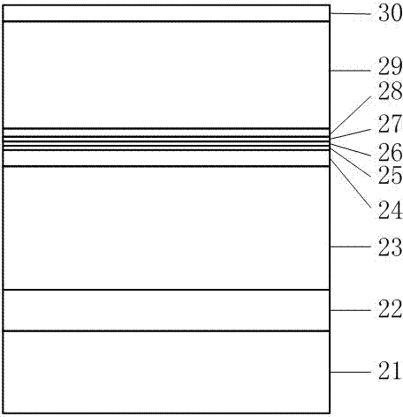
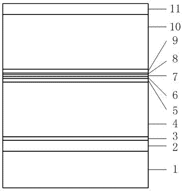
[0085] 1. Preparation of epitaxial wafers:

[0086] The present invention adopts metal organic compound vapor phase epitaxy (MOCVD) equipment produced by AIXTRON company, and the processing steps are as follows:

[0087] 1) With (100) GaAs with a 15-degree bias to the direction as the substrate, SiH is introduced 4 , the thickness of the grown GaAs buffer layer reaches 100nm;

[0088] 2) A transition layer is grown on the GaAs buffer layer, and the material is Al x Ga 1-x As, among them, x 0.3~0.7, the growth thickness of the transition layer is 300nm, SiH is introduced during growth 4 , the Si doping concentration of this epitaxial layer is 1×10 18 cm -3 ;

[0089] 3) On the transition layer, with Al 0.7 Ga 0.3 As is the material, the n-type lower confinement layer is grown, the growth thickness is 1500nm, and SiH is introduced during the growth 4 , the Si doping concentration of this epitaxial layer is 1×10 18 cm -3 ;

[0090] 4) A lower waveguide layer with a...


PUM


Abstract

The invention discloses an epitaxial wafer for a 980nm F-P cavity strained quantum well laser with a narrow line width and a preparation method of the epitaxial wafer for the 980nm F-P cavity strained quantum well laser with the narrow line width, and relates to the field of a semiconductor laser. A growth buffer layer, a transition layer, a n-type lower restriction layer, a lower waveguide layer, a lower potential barrier layer, an active layer, an upper potential barrier layer, an upper waveguide layer, a p-type upper restriction layer and an ohmic contact layer are grown on a GaAs substrate layer in sequence so as to be processed into the 980nm F-P cavity strained quantum well laser with the narrow line width. The epitaxial wafer for the 980nm F-P cavity strained quantum well laser with the narrow line width can be applied to the fields, such as optical measurement, solid laser pumping, laser spectroscopy, medical research and the like.

Description

technical field [0001] The invention relates to the field of semiconductor lasers, in particular to a low line width F-P cavity strain quantum well laser emitting 980nm wavelength. Background technique [0002] 980nm semiconductor lasers are widely used in communication and medical fields. It is the window of the pump source of erbium-doped fiber amplifiers and the preferred wavelength for laser scalpels. Quantum well laser is a new type of semiconductor laser developed in recent years. Since the thickness of the active layer is smaller than the mean free path of electrons, the carriers can only move in the active layer, which improves the conversion efficiency of the laser. [0003] Line width expansion factor (Linewidth Enhancement Factor, factor) is an important factor affecting the spectral line width of semiconductor lasers. It not only directly affects the spectral linewidth of the semiconductor laser, but also affects the mode stability of the laser, the chirp und...

Claims


Application Information

Patent Timeline
Patent Type & Authority Applications(China)
IPC IPC(8): H01S5/343H01S5/14
Inventor 张帆韩效亚杜石磊林晓珊叶培飞占荣耿松涛张双翔
Owner YANGZHOU CHANGELIGHT
Why Eureka
Try Eureka