Array substrate and manufacturing method thereof as well as display equipment

A manufacturing method and array substrate technology, applied in the fields of array substrate, display device, and array substrate manufacturing, can solve the problems of high manufacturing cost and achieve the effect of reducing manufacturing cost

Inactive Publication Date: 2012-11-21
BOE TECH GRP CO LTD
View PDF5 Cites 52 Cited by
  • Summary
  • Abstract
  • Description
  • Claims
  • Application Information

AI Technical Summary

Problems solved by technology

[0013] This method requires 6 patterning pr...

Method used


Image

  • Array substrate and manufacturing method thereof as well as display equipment
  • Array substrate and manufacturing method thereof as well as display equipment
  • Array substrate and manufacturing method thereof as well as display equipment

Examples


Embodiment 1

[0043] The method for manufacturing an array substrate provided by an embodiment of the present invention includes a manufacturing process of a thin film transistor, a first transparent electrode, and a second transparent electrode. The first transparent electrode and the second transparent electrode generate a multidimensional electric field. Wherein, the manufacturing process of the first transparent electrode includes:

[0044] Step 1: forming a metal oxide film, which has semiconductor properties.

[0045] Step 2: forming a first transparent electrode by performing metallization treatment on part of the metal oxide thin film, and forming a semiconductor active layer on the part not subjected to the metallization treatment.

[0046] Further, in step 2, "forming the first transparent electrode by performing metallization treatment on part of the metal oxide film" may specifically include: performing metallization treatment on part of the metal oxide film through a plasma pr...

Embodiment 2

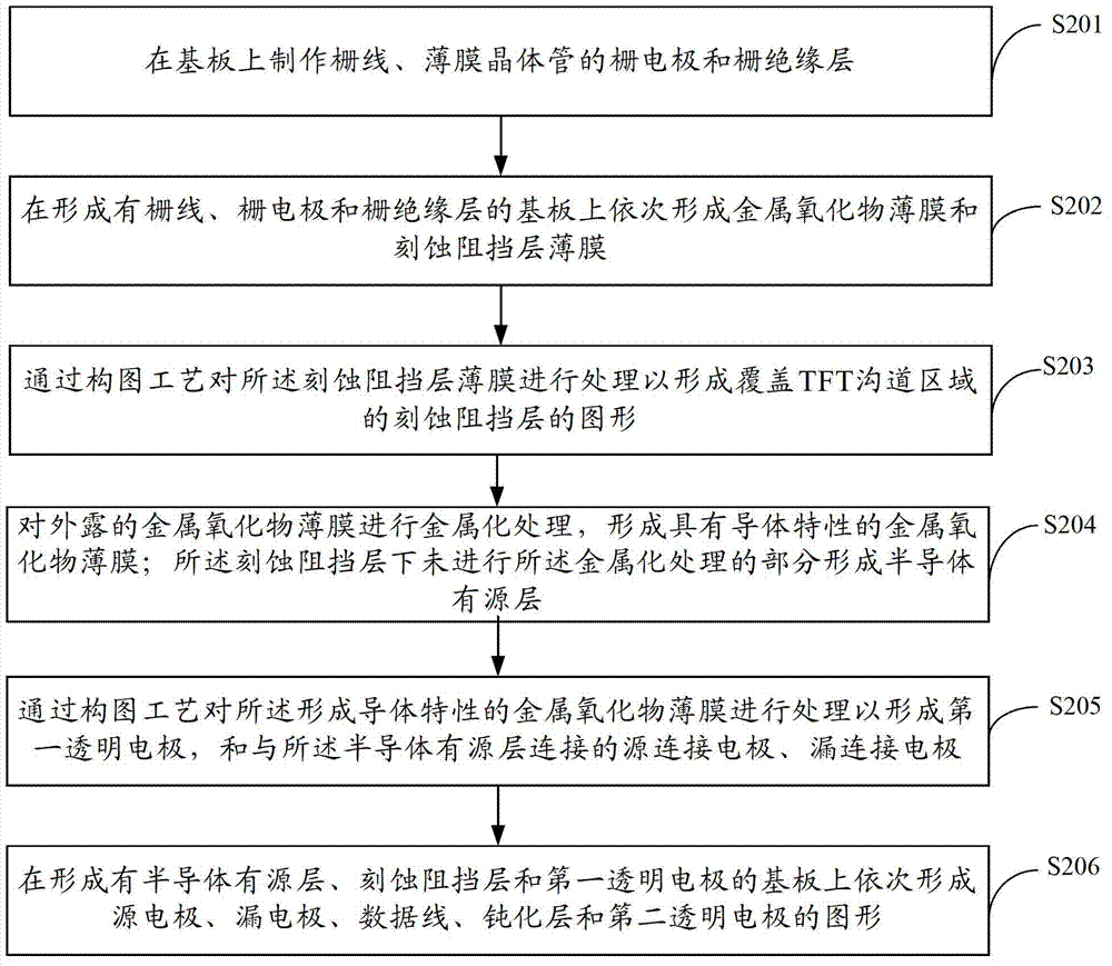
[0050] The manufacturing method of the array substrate provided by the embodiment of the present invention, such as figure 2 As shown, the method specifically includes:

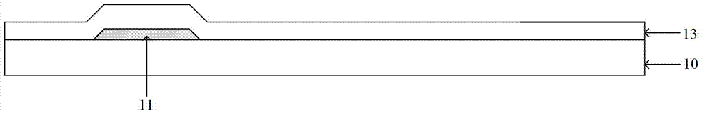
[0051] S201 , fabricating a gate line, a gate electrode and a gate insulating layer of a thin film transistor on a substrate.

[0052] Exemplary, see image 3 Firstly, a first metal thin film is formed on the substrate 10 (such as a glass substrate or a quartz substrate) by plasma enhanced chemical vapor deposition (PECVD), magnetron sputtering, thermal evaporation or other film forming methods. Wherein, the first metal thin film may be a single-layer thin film formed of metals such as molybdenum, aluminum, aluminum-rubidium alloy, tungsten, chromium, copper, etc., or a multi-layer thin film formed by multi-layer deposition of the above metals. After the photoresist layer is coated on the first metal film, patterning processes such as exposure, development, etching and stripping are carried out through a mas...

Embodiment 3

[0074] The basic process of the manufacturing method of the array substrate provided by the embodiment of the present invention is similar to that of the second embodiment, and reference may be made to the second embodiment.

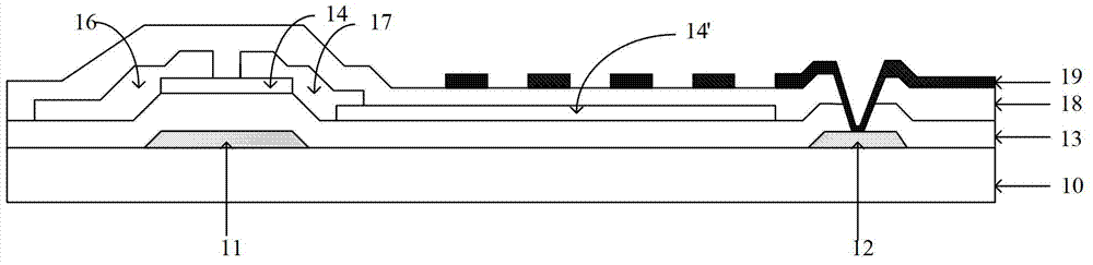
[0075] The difference between this embodiment and Embodiment 2 is that, relative to S201 of Embodiment 2, S201' of this embodiment includes: Figure 13 As shown, gate lines are formed on the substrate 10 ( Figure 13 (not shown in ), gate electrode 11 , common electrode line 12 is also formed, and then gate insulating layer 13 is formed on substrate 10 .

[0076] Further, the common electrode lines 12, the gate electrodes 11 and the gate lines can be formed through one patterning process.

[0077] The steps after forming the gate lines, gate electrodes and common electrode lines are the same as the steps S202-S205 in the second embodiment, and will not be repeated here.

[0078] Patterns of source electrodes, drain electrodes, data lines, passivation l...


PUM


Abstract

The embodiment of the invention discloses an array substrate and a manufacturing method thereof as well as display equipment, which belong to the technical field of liquid crystal displays and are used for lowering manufacturing cost. The manufacturing method comprises manufacturing processes of a film transistor, a first transparent electrode and a second transparent electrode; the first and the second transparent electrodes generate a multi-dimensional electric field; the manufacturing process of the first transparent electrode comprises formation of a metallic oxide film which has characteristics of a semiconductor; and the first transparent electrode is formed via a metalizing process of a part of the metallic oxide film, a semi-conductor active layer is formed by the rest of the metallic oxide film, which is executed for metalizing process. The manufacturing method disclosed by the embodiment of the invention is applicable to manufacturing of the liquid crystal displays.

Description

technical field [0001] The invention relates to the technical field of liquid crystal display, in particular to a method for manufacturing an array substrate, the array substrate, and a display device. Background technique [0002] A liquid crystal display is a commonly used flat panel display at present, and a Thin Film Transistor Liquid Crystal Display (TFT-LCD for short) is a mainstream product in the liquid crystal display. [0003] TFT-LCD based on ADvanced Super Dimension Switch (AD-SDS, ADS for short) is more and more widely used due to its low power consumption, wide viewing angle and other characteristics. ADS technology mainly forms a multi-dimensional electric field through the electric field generated by the edge of the slit electrode in the same plane and the electric field generated between the slit electrode layer and the plate electrode layer, so that all aligned liquid crystal molecules between the slit electrodes and directly above the electrodes in the liq...

Claims


Application Information

Patent Timeline
IPC IPC(8): H01L21/77
CPCH01L21/77H01L27/1225H01L21/02664H01L29/7869H01L21/02565H01L27/1203G02F1/134363G02F1/134372G02F1/136231G02F1/134309G02F1/13439H01L29/66742H01L29/66969
Inventor 崔承镇金熙哲宋泳锡刘聖烈
Owner BOE TECH GRP CO LTD
Why Eureka
Try Eureka