Polycrystalline silicon film, preparation method thereof, array substrate and display device

A polysilicon thin film and display device technology, which is applied in semiconductor/solid-state device manufacturing, semiconductor devices, electrical components, etc., can solve the problem of poor repeatability, stability, and uniformity of polysilicon thin films, poor characteristics of polysilicon thin films, and excimer laser energy density. Difficult to control and other issues

Active Publication Date: 2013-01-02
BOE TECH GRP CO LTD
View PDF7 Cites 16 Cited by
  • Summary
  • Abstract
  • Description
  • Claims
  • Application Information

AI Technical Summary

Problems solved by technology

The crystal grains of polysilicon formed by these methods are quite small, so the properties of polysilicon films formed by these methods are not good
At present, in the production of polysilicon thin films, the most commonly used excimer laser annealing method is a low-temperature polysilicon thin film production technology, but since the excimer laser is a pulsed laser, the energy density of each pulse will be differen

Method used


Image

  • Polycrystalline silicon film, preparation method thereof, array substrate and display device
  • Polycrystalline silicon film, preparation method thereof, array substrate and display device
  • Polycrystalline silicon film, preparation method thereof, array substrate and display device

Examples


preparation example Construction

[0026] A first aspect of the present invention provides a method for preparing a polysilicon film, comprising the following steps:

[0027] (1) forming a graphene layer and an amorphous silicon layer, wherein the graphene layer and the amorphous silicon layer are adjacent;

[0028] (2) Crystallize amorphous silicon to form polysilicon to obtain a polysilicon film.

[0029] The polysilicon in the polysilicon thin film prepared by the method has the advantages of no pollution and low defect density, and the obtained polysilicon has uniform grain size, orderly arrangement and large grain size, and better surface flatness. The polysilicon thin film prepared by the method has good repeatability, stability and uniformity, can be crystallized in a large area, and can meet the requirement of producing high-performance polysilicon materials.

specific Embodiment approach 1

[0031] This embodiment provides a method for preparing a polysilicon thin film, comprising the following steps:

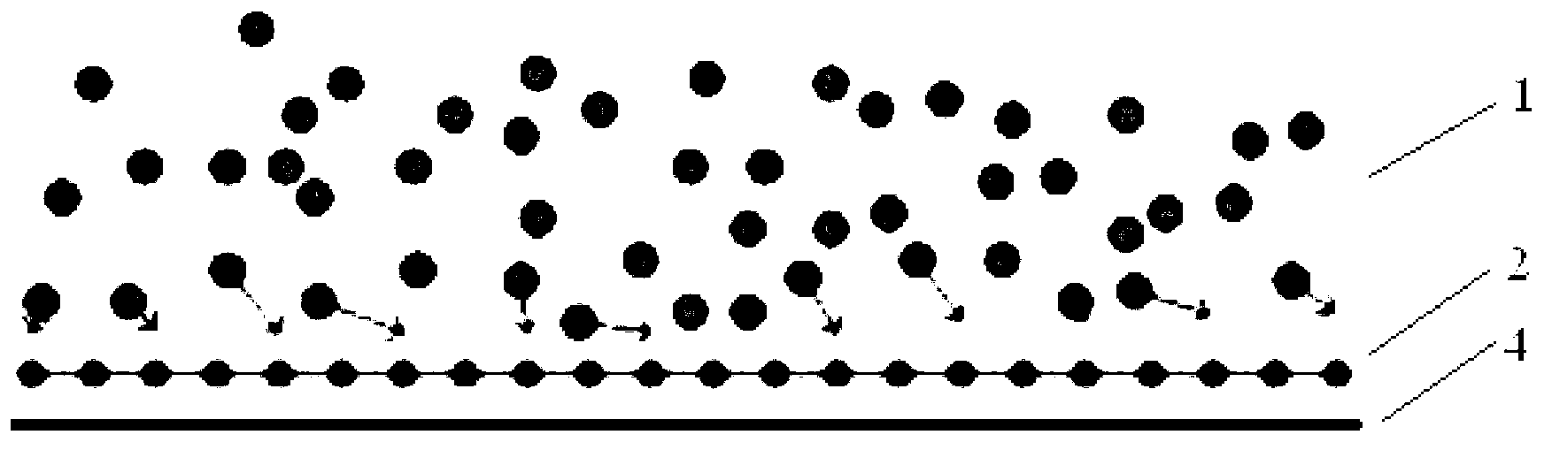
[0032] (1) The base layer 4 of the polysilicon thin film is formed. The formation of the base layer 4 of the polysilicon thin film is an existing known technology, which can include: firstly provide a substrate, this substrate is usually a glass substrate, certainly this substrate can also be a plastic substrate or other transparent substrates, However, the substrate may also be other opaque substrates, such as silicon substrates. Then a buffer layer is formed on the substrate, and the buffer layer is usually composed of a barrier layer and a stress buffer layer. Among them, the barrier layer is usually a silicon nitride layer, and the silicon nitride layer is usually formed by chemical vapor deposition; and the stress buffer layer is usually silicon oxide, and the silicon oxide layer is usually formed by chemical vapor deposition. , the film structure is relativ...

specific Embodiment approach 2

[0042] This specific embodiment provides a kind of preparation method of polysilicon film, comprises the following steps:

[0043] (1) The manufacturing method of the base layer in this embodiment is as in Embodiment 1.

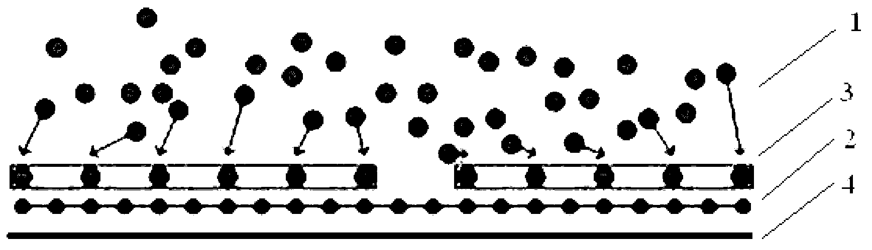
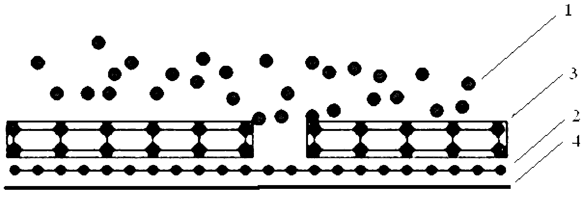
[0044] (2) An amorphous silicon layer with a thickness of preferably 40-50 nanometers is formed on the base layer, and a graphene layer with a thickness of preferably 2-10 layers is formed on the amorphous silicon layer. Wherein, the formation method of the amorphous silicon layer and the formation method of the graphene layer are the same as those in the first embodiment.

[0045] (3) Crystallize amorphous silicon to form polysilicon by excimer laser annealing method, and obtain polysilicon thin film. The crystallization method used in this step is the same as that in Embodiment 1. Graphene crystals can be produced on a large scale, and the crystal quality is very high. Since the thickness of the graphene prepared in the polysilicon film production process...


PUM

PropertyMeasurementUnit
Thicknessaaaaaaaaaa
Sizeaaaaaaaaaa

Abstract

The invention discloses a polycrystalline silicon film and a preparation method thereof, an array substrate and a display device, belonging to the technical field of semiconductors. The preparation method of the polycrystalline silicon film comprises the following steps of: (1) forming a graphene layer and a noncrystalline silicon layer which are adjacent; and (2) enabling noncrystalline silicon to crystallize and form polycrystalline silicon and obtaining the polycrystalline silicon film. The polycrystalline silicon in the polycrystalline silicon film has the advantages of no pollution and low defect density, the crystal grain size of the polycrystalline silicon is uniform in size, the arrangement is ordered, the crystal grain is larger, and further the surface flatness is better. The speed rate of current carriers in the polycrystalline silicon film prepared by the method is increased, and the element performance of a polycrystalline silicon film transistor is improved.

Description

technical field [0001] The invention belongs to the technical field of semiconductors, and in particular relates to a polysilicon thin film, a preparation method thereof, an array substrate, and a display device. Background technique [0002] Polycrystalline silicon thin film is a new type of functional material that combines the advantages of crystalline silicon and amorphous silicon materials. The study of materials has attracted more and more attention. [0003] Polysilicon thin film is composed of many small crystal grains with different sizes and crystal plane orientations. The grain size is generally between tens and hundreds of nanometers, and the large grain size can reach several microns. Large-grain polysilicon thin films have higher mobility, which is close to that of bulk materials, so polysilicon thin films have been widely used in the manufacture of semiconductor devices, such as polysilicon thin film transistors (TFT, Thin Film Transisitor) for display indust...

Claims


Application Information

Patent Timeline
IPC IPC(8): H01L21/20H01L27/12H01L27/32
CPCH01L27/1277H01L29/78603H01L29/6675H01L21/02595H01L21/02667H01L21/02675
Inventor 孙拓
Owner BOE TECH GRP CO LTD
Why Eureka
Try Eureka