Stress regulated semiconductor and associated methods
A technology of stress adjustment and semiconductor, applied in the field of electronics and materials science, can solve problems such as limitations, limitations of electronic devices, and increased volume of cooling devices
- Summary
- Abstract
- Description
- Claims
- Application Information
AI Technical Summary
Problems solved by technology
Method used
Image

Examples
Embodiment 1
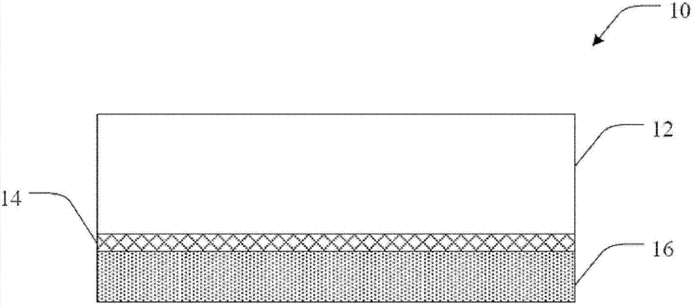
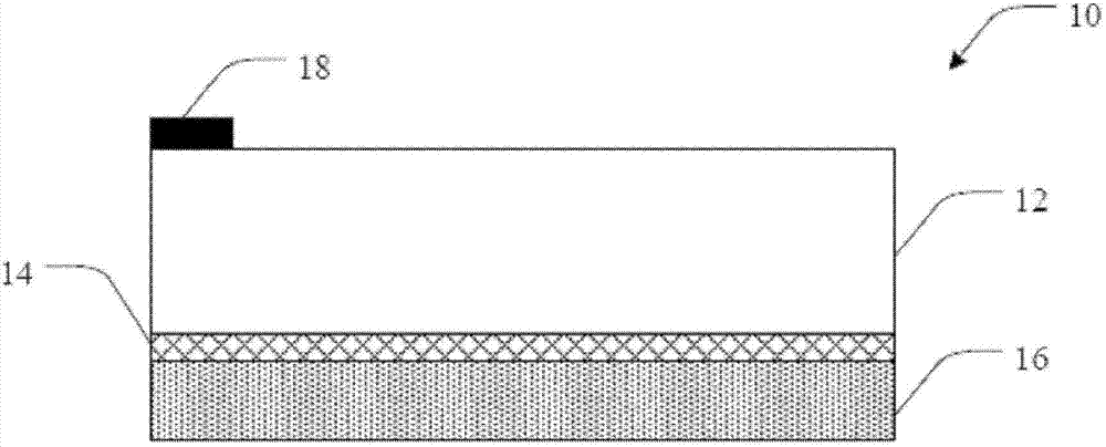
[0077] Epitaxial GaN is formed on a sapphire wafer by MOCVD (Metal Organic Chemical Vapor Deposition). Next, trimethylgallium is used as the source gas of Ga, ammonia is added to provide nitrogen atoms, and hydrogen can be added to dilute the gas and vaporize Ga or N atoms that are unstablely arranged in the crystal lattice. A multilayer semiconductor structure formed with n-type dopants containing silicon forms a junction with a sapphire substrate formed with p-type dopants containing Mg. The quantum well and intrinsic layer can be disposed between the p-type doped layer and the n-type doped layer. Next, an Ag reflective layer with a thickness of about 200 nm is sputtered on the top surface of the p-type doped layer, and then a Ti nucleation enhancer layer with a thickness of about 50 nm is sputtered on the reflective layer.
[0078] Next, deposit amorphous diamond with a thickness of about 1 μm on the nucleation enhancer layer by cathodic arc deposition. Another Ti nucleat...
Embodiment 2
[0080] Epitaxial GaN is formed on a sapphire wafer by MOCVD (Metal Organic Chemical Vapor Deposition). Trimethylgallium is the source gas of Ga, and ammonia is added to supply nitrogen atoms, and hydrogen can be added to dilute the gas and vaporize Ga or N atoms that are unstablely arranged in the crystal lattice. A multilayer semiconductor structure formed from n-type dopants containing silicon forms a junction with a sapphire wafer formed from p-type dopants containing Mg. The quantum well and the intrinsic layer can be arranged between the p-type doped layer and the n-type doped layer.
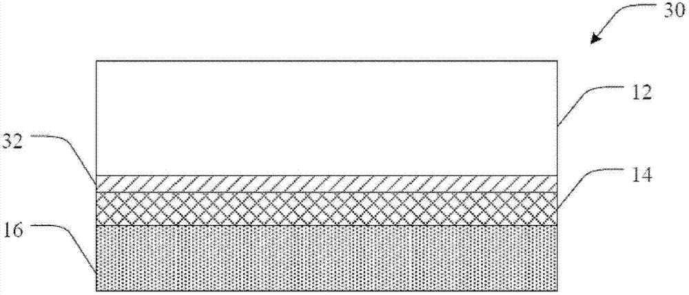
[0081] On the top surface of the p-type doped layer, graphite and Au are co-sputtered to form a reflective layer, wherein graphite is used to reduce the CTE of the reflective layer. In this case, CTE can be graded by controlling the ratio of Ag / C. Next, continue to coat graphite-free Ag on the reflective layer, and thicken the Ag layer by electroplating Cu or Ag.
Embodiment 3
[0083] Epitaxial GaN is formed on a sapphire wafer by MOCVD (Metal Organic Chemical Vapor Deposition). Trimethylgallium is the source gas of Ga, and ammonia is added to supply nitrogen atoms, and hydrogen can be added to dilute the gas and vaporize Ga or N atoms that are unstablely arranged in the crystal lattice. A multilayer semiconductor structure formed from n-type dopants containing silicon forms a junction with a sapphire wafer formed from p-type dopants containing Mg. The quantum well and the intrinsic layer can be arranged between the p-type doped layer and the n-type doped layer.
[0084]On the top surface of the p-type doped layer, graphite and Au are co-sputtered to form a reflective layer, wherein graphite is used to reduce the CTE of the reflective layer. In this case, CTE can be graded by controlling the ratio of Ag / C. Next, continue to coat graphite-free Ag on the reflective layer. A micron-sized monolayer of diamond particles is coated on the Ag layer, and t...
PUM
| Property | Measurement | Unit |
|---|---|---|
| Thermal expansion coefficient | aaaaa | aaaaa |
| Size | aaaaa | aaaaa |
| Thickness | aaaaa | aaaaa |
Abstract
Description
Claims
Application Information
 - R&D
- Intellectual Property
- Life Sciences
- Materials
- Tech Scout
- Unparalleled Data Quality
- Higher Quality Content
- 60% Fewer Hallucinations
Browse by: Latest US Patents, China's latest patents, Technical Efficacy Thesaurus, Application Domain, Technology Topic, Popular Technical Reports.
© 2025 PatSnap. All rights reserved.Legal|Privacy policy|Modern Slavery Act Transparency Statement|Sitemap|About US| Contact US: help@patsnap.com