
Silicon carbide crystal growth crucible for increasing utilization rate of power sources

A crystal growth, silicon carbide technology, applied in the direction of crystal growth, single crystal growth, single crystal growth, etc., can solve the problems of low utilization rate of silicon carbide powder source, low average crystal growth rate, etc., to reduce the phenomenon of secondary crystallization , the effect of improving the utilization rate and the average growth rate of the crystal, and increasing the temperature of the powder source

Active Publication Date: 2013-02-06
XIAN UNIV OF TECH
View PDF1 Cites 3 Cited by
  • Summary
  • Abstract
  • Description
  • Claims
  • Application Information

AI Technical Summary

Problems solved by technology

[0006] The purpose of the present invention is to provide a silicon carbide crystal growth crucible for improving the utilization rate of powder source, which solves the problems of low utilization rate of silicon carbide powder source and low average crystal growth rate in the prior art

Method used


Image

  • Silicon carbide crystal growth crucible for increasing utilization rate of power sources
  • Silicon carbide crystal growth crucible for increasing utilization rate of power sources
  • Silicon carbide crystal growth crucible for increasing utilization rate of power sources

Examples


Embodiment 1

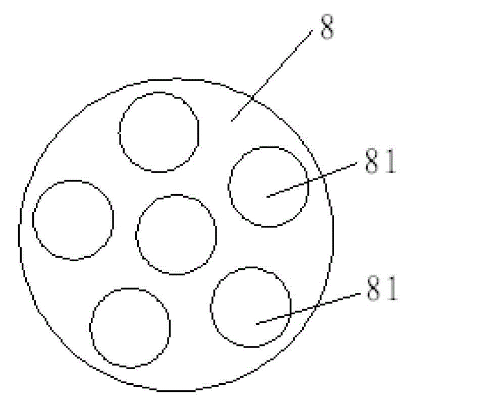
[0017] Such as figure 2 As shown, the present invention includes a crucible body 8 whose external shape is cylindrical and made of graphite. The cross-sections of the regions 81 are all circular and are evenly arranged in a honeycomb shape in the horizontal direction, specifically: one of the circular subpackaging regions 81 is located at the center of the crucible body 8, and the other five are distributed circumferentially outside it. The crucible body 8 has an integrated structure, that is, the intervals between the five sub-packaging regions 81 are of the same material and integrated structure, which is conducive to reducing the radial temperature gradient of the silicon carbide source.

Embodiment 2

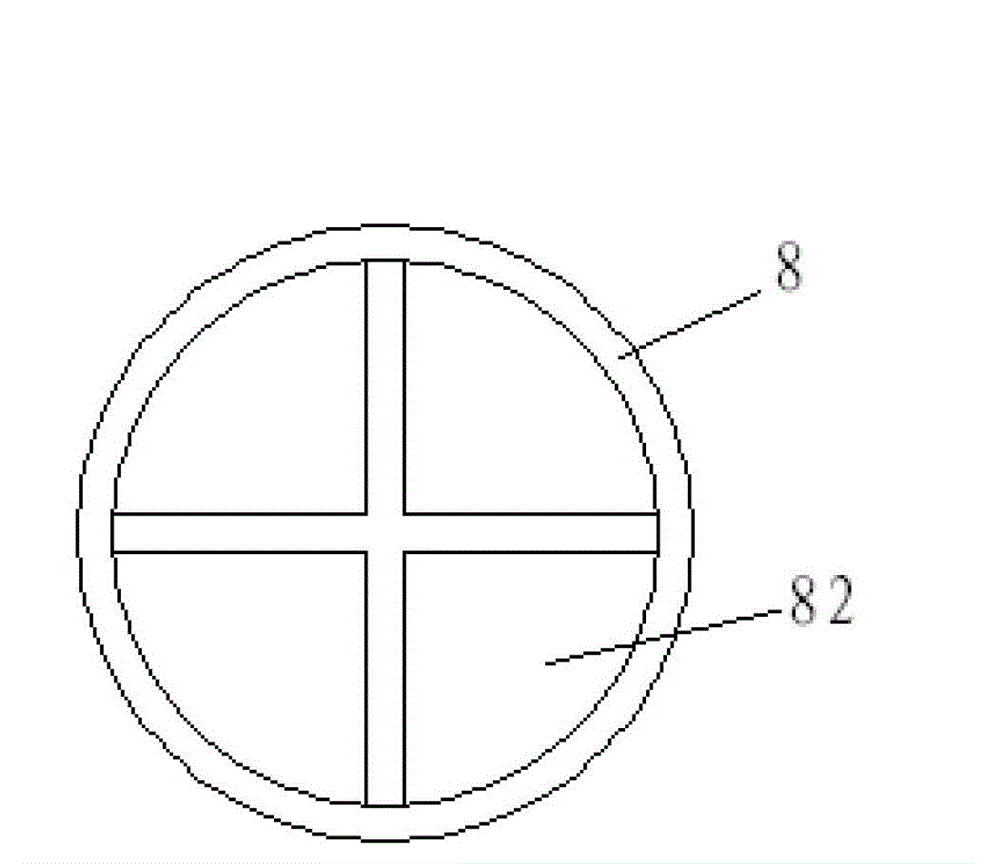
[0019] Such as image 3 As shown, the present invention includes a crucible body 8 whose external shape is cylindrical and made of graphite. The inner cavity of the crucible body includes four fan-shaped sub-package areas 82 for containing silicon carbide powder sources. The four fan-shaped sub-package areas 82 The cross-sections are fan-shaped and distributed along the center and circumference of the crucible body in the horizontal direction. The crucible body 8 has an integrated structure, that is, the intervals between the four fan-shaped sub-packaging regions 82 are of the same material and integrated structure, which is beneficial to reduce the radial temperature gradient of the silicon carbide source.

[0020] In the present invention, a crucible with an unreasonable inner cavity partition form is selected according to needs, and the shape and number of subpackage areas in the crucible inner cavity are determined according to the requirements of the working conditions, s...


PUM


Abstract

The invention discloses a silicon carbide crystal growth crucible for increasing utilization rate of power sources and solves the problems that utilization rate of silicon carbide power sources is low and average growth rate of crystal is low. The silicon carbide crystal growth crucible comprises a crucible body. A cavity of the crucible body is divided into a plurality of split areas for containing silicon carbide power sources horizontally.

Description

technical field [0001] The invention belongs to the technical field of artificial crystal growth, and in particular relates to a silicon carbide crystal growth crucible for improving the utilization rate of powder sources. Background technique [0002] The third-generation semiconductor material silicon carbide (SiC) has the characteristics of wide band gap, high critical avalanche breakdown electric field strength, high electron saturation drift velocity, high thermal conductivity, high temperature resistance, radiation resistance and corrosion resistance. Electronic devices, high-power solid-state microwave devices, solid-state sensors and other new devices, as well as the preferred materials for high-temperature-resistant integrated circuits, are widely used in petroleum, chemical, automotive, aviation, aerospace, communications, weapons and other industries. [0003] Silicon carbide has no liquid phase under normal engineering conditions, and begins to sublime into gas a...

Claims


Application Information

Patent Timeline
IPC IPC(8): C30B29/36C30B35/00C30B23/00
Inventor 封先锋陈治明臧源马剑平蒲红斌
Owner XIAN UNIV OF TECH
Learn More