Graphical silicon carbide (SiC) substrate

A patterning and substrate technology, applied in chemical instruments and methods, from chemically reactive gases, crystal growth, etc., can solve the problems of affecting the crystalline quality of thin films, unable to bond firmly to the substrate, etc., to reduce the linear dislocation density, The effect of improving performance and stability

Inactive Publication Date: 2013-02-13
SHANGHAI INST OF TECH
View PDF1 Cites 8 Cited by
  • Summary
  • Abstract
  • Description
  • Claims
  • Application Information

AI Technical Summary

Problems solved by technology

Defects such as stress, strain, and dislocations caused by lattice mismatch will affect the crystalline quality of the film, and even cannot be firmly bonded to the substrate

Method used


Image

  • Graphical silicon carbide (SiC) substrate
  • Graphical silicon carbide (SiC) substrate
  • Graphical silicon carbide (SiC) substrate

Examples


Embodiment 1

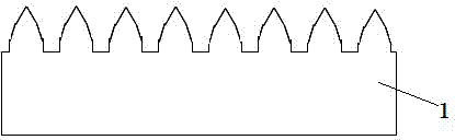
[0039] As shown in FIG. 5 , the pattern structure described in the embodiment of the present invention is a triangular pyramid, the bottom surface of the pattern is 2.4 μm in size, the distance between adjacent patterns is 0.6 μm, and the pattern height is 1.5 μm.

Embodiment 2

[0041]As shown in FIG. 6 , the graphic structure described in the embodiment of the present invention is a spherical cap graphic, the size of the bottom surface of the graphic is 3.3 μm, the distance between adjacent graphics is 0.3 μm, and the graphic height is 1.2 μm.

Embodiment 3

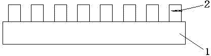
[0043] As shown in FIG. 7 , the pattern structure described in the embodiment of the present invention is a cylindrical pattern, the bottom surface of the pattern is 1.2 μm in size, the distance between adjacent patterns is 1.1 μm, and the pattern height is 2 μm.


PUM

PropertyMeasurementUnit
diameteraaaaaaaaaa
heightaaaaaaaaaa
thicknessaaaaaaaaaa

Abstract

The invention relates to a graphical silicon carbide (SiC) substrate. The surface of the graphical SiC substrate comprises periodized protrusions or concave images which are formed by means of plasma etching or wet etching, wherein the periodized protrusions or the concave images are any one of multilateral cones, multilateral cylinders, multi-rowed frustums, trapezoid multilateral frustums, trapezoid round pedestals, hemispheres or spherical crowns. Periodic images are combination of any two or more than two of the multilateral cones, the multilateral cylinders, the multi-rowed frustums, the trapezoid multilateral frustums, the trapezoid round pedestals, the hemispheres or the spherical crowns. The graphical SiC substrate can improve epitaxy quality of heteroepitaxy of gallium nitride (GaN) and homoepitaxy of 3C-SiC which take SiC as the substrate, and improves performance and stability of elements prepared by epitaxial wafers.

Description

technical field [0001] The invention relates to a silicon carbide (SiC) substrate for heteroepitaxial growth of GaN epitaxial wafers and homoepitaxial growth of 3C-SiC epitaxial wafers. Background technique [0002] Wide bandgap semiconductor materials represented by 3C-SiC (silicon carbide) and GaN (gallium nitride) have large bandgap width, high breakdown electric field, high thermal conductivity, high electron saturation drift velocity, strong radiation resistance and Good chemical stability and other superior properties have become the key semiconductor materials for manufacturing a new generation of microelectronic devices and circuits after germanium (Ge), silicon (Si), and gallium arsenide (GaAs). Wide bandgap semiconductor materials have unique advantages in making microwave high-power devices, high-temperature-resistant devices and radiation-resistant devices. They are ideal materials for realizing the combination of microwave and high-power, high-temperature and ra...

Claims


Application Information

Patent Timeline
Patent Type & Authority Applications(China)
IPC IPC(8): C30B25/18
Inventor 储耀卿
Owner SHANGHAI INST OF TECH
Why Eureka
Try Eureka