

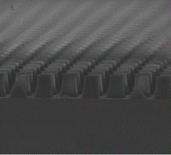
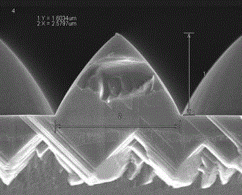
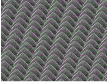
Photoetching method of graphical sapphire substrate
A technology for patterning sapphire and substrates, which is applied in microlithography exposure equipment, photolithography process of pattern surface, optics, etc., can solve the problems of poor pattern consistency, low product qualification rate, and high linear dislocation density, and achieves The effect of high finished product qualification rate and yield, accurate pattern size and low linear dislocation density
- Summary
- Abstract
- Description
- Claims
- Application Information
AI Technical Summary
Problems solved by technology
Method used
Image

Examples
Embodiment 1
[0020] A kind of photolithography method of patterned sapphire substrate that the present invention proposes, comprises the following steps:
[0021] S1. Using plasma-enhanced chemical vapor deposition technology to deposit a layer of SiO on a patterned sapphire substrate 2 film, and use high-pressure nitrogen blowing method to remove the particles on the surface of the film, and perform low-temperature drying treatment;
[0022] S2. When the rotation speed is 5000RPM and the rotation acceleration is constant, drop liquid photoresist and tackifier into the middle of the substrate film layer at a mass ratio of 1:0.05, and use centrifugal force to place the liquid photoresist Evenly cover the surface of the wafer, and then put the substrate with photoresist on the hot plate for baking, the baking temperature is 100°C, and the baking time is 40s to form a photoresist film with a thickness of 1 μm;
[0023] S3. Keep the distance between the mask plate and the substrate at 3cm, pr...
Embodiment 2
[0026] A kind of photolithography method of patterned sapphire substrate that the present invention proposes, comprises the following steps:
[0027] S1. Using plasma-enhanced chemical vapor deposition technology to deposit a layer of Si on a patterned sapphire substrate 3 N 4 film, and use chemical wet cleaning method to remove the particles on the surface of the film, and perform low-temperature drying treatment;
[0028] S2. When the rotation speed is 3000RPM and the rotation acceleration is constant, drop liquid photoresist and tackifier into the middle of the substrate film layer at a mass ratio of 1:0.02, and use centrifugal force to place the liquid photoresist Evenly cover the surface of the wafer, and then put the substrate with photoresist on the hot plate for baking, the baking temperature is 90°C, and the baking time is 60s to form a photoresist film with a thickness of 0.8 μm;
[0029] S3. Keep the distance between the mask plate and the substrate at 2.5cm, proj...
Embodiment 3
[0032] A kind of photolithography method of patterned sapphire substrate that the present invention proposes, comprises the following steps:
[0033] S1. Using plasma-enhanced chemical vapor deposition technology, a layer of Ni film is deposited on a patterned sapphire substrate, and the particles on the surface of the film are removed by high-pressure nitrogen blowing method, and low-temperature drying is performed;
[0034] S2. When the rotation speed is 6000RPM and the rotation acceleration is constant, drop liquid photoresist and tackifier into the middle of the substrate film layer at a mass ratio of 1:0.06, and use centrifugal force to place the liquid photoresist Evenly cover the surface of the wafer, and then put the substrate with photoresist on the hot plate for baking, the baking temperature is 80°C, and the baking time is 90s, forming a photoresist film with a thickness of 1.2 μm;
[0035] S3. Keep the distance between the mask plate and the substrate at 4cm, proje...
PUM
 Abstract
Description
Claims
Application Information