

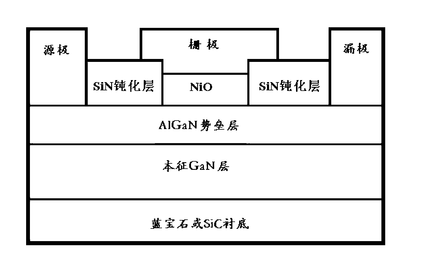
AlGaN/GaN heterojunction enhanced device and manufacturing method thereof
A manufacturing method and enhanced technology, applied in the field of microelectronics, can solve problems such as poor process repeatability and poor voltage uniformity, and achieve the effects of good controllability, increased forward threshold voltage, and reduced two-dimensional electron gas density
- Summary
- Abstract
- Description
- Claims
- Application Information
AI Technical Summary
Problems solved by technology
Method used
Image

Examples
Embodiment 1
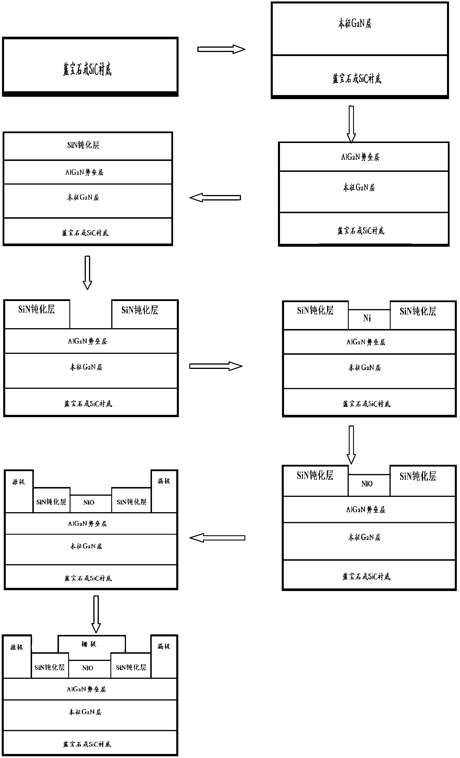
[0033] The manufacture of the device of the present invention includes the following steps:
[0034] step 1. Epitaxial material growth.
[0035] 1.1) On the SiC substrate, use the MOCVD process to grow the intrinsic GaN layer;
[0036] 1.2) On the intrinsic GaN layer, grow an 8nm thick AlGaN barrier layer, in which the Al composition is 35%,
[0037] A 2DEG is formed at the contact position between the intrinsic GaN layer and the AlGaN barrier layer to obtain a sample with epitaxial material.
[0038] Step 2. Made of NiO under the gate.
[0039] 2.1) Use PECVD790 deposition equipment to deposit SiN on the AlGaN barrier layer, and deposit SiN with a thickness of 50 nm;
[0040] 2.2) SiN gate trench etching;
[0041] First, slant the glue on the surface of the epitaxial material at a speed of 5000 rpm to obtain a photoresist mask with a thickness of 0.8 μm, and then bake it in a high-temperature oven with a temperature of 80 ° C for 10 minutes, and then use the NSR1755I7A ...
Embodiment 2
[0065] Step 1. On the SiC substrate, use the MOCVD process to grow an intrinsic GaN layer; then on the intrinsic GaN layer, grow an AlGaN barrier layer with a thickness of 12 nm and an Al composition of 30%, and on the intrinsic GaN layer. A 2DEG is formed at the contact position with the AlGaN barrier layer, and a sample with epitaxial material is obtained.
[0066] Step 2, making NiO under the gate.
[0067] 2a) Using PECVD790 deposition equipment to deposit a 100nm SiN layer on the AlGaN barrier layer;
[0068] 2b) Spin the glue on the surface of the epitaxial material at a speed of 5000 rpm to obtain a photoresist mask with a thickness of 0.8 μm, and then bake it in a high temperature oven with a temperature of 80 ° C for 10 minutes, and obtain it by lithography using an NSR1755I7A lithography machine. Gate electrode pattern; then use ICP98c inductively coupled plasma etcher to etch and remove the 100nm thick SiN layer in the gate area at an etching rate of 0.5nm / s to for...
Embodiment 3
[0077] step a. Epitaxial material growth.
[0078] A1) On the sapphire substrate, use the MOCVD process to grow the intrinsic GaN layer;
[0079] A2) On the intrinsic GaN layer, grow a 16nm thick AlGaN barrier layer, in which the Al composition is 25%,
[0080] A 2DEG is formed at the contact position between the intrinsic GaN layer and the AlGaN barrier layer to obtain a sample with epitaxial material.
[0081] Step B. Made of NiO under the grid.
[0082] B1) Deposit SiN on the AlGaN barrier layer using PECVD790 deposition equipment, and deposit SiN with a thickness of 200nm;
[0083] B2) SiN gate groove etching;
[0084] First, the positive resist was cast on the surface of the epitaxial material at a speed of 5000 rpm to obtain a photoresist mask with a thickness of 0.8 μm, and then baked in a high-temperature oven at a temperature of 80°C for 10 minutes, and then photolithography was carried out using an NSR1755I7A photolithography machine. Obtain the gate electrode ...
PUM
| Property | Measurement | Unit |
|---|---|---|
| Thickness | aaaaa | aaaaa |
| Thickness | aaaaa | aaaaa |
| Thickness | aaaaa | aaaaa |
Abstract
Description
Claims
Application Information