Compensation method for increase of amplification times of direct current caused by thinning of germanium-silicon edge

A technology of DC current and compensation method, applied in the manufacturing of circuits, electrical components, semiconductor/solid-state devices, etc., can solve problems such as yield drop, achieve yield improvement, compensate for the rise of collector current, and tighten the distribution of magnification. Effect

Active Publication Date: 2015-06-03
SHANGHAI HUAHONG GRACE SEMICON MFG CORP
View PDF4 Cites 0 Cited by
  • Summary
  • Abstract
  • Description
  • Claims
  • Application Information

AI Technical Summary

Problems solved by technology

Its advantage is that the process is simple, and the mask layer can be reduced by half compared with the traditional process. The disadvantage is that when silicon germanium is grown on the optical wafer, the thickness of the silicon germanium epitaxial layer will drop sharply from the edge of the wafer about 12mm. The thickness of each layer of the silicon germanium epitaxial layer will be lower than the center, and the thickness difference can reach up to 20%. This is due to the combined effect of the design of the heating method of the epitaxial equipment and the heat conduction of the light sheet.
Since the collector current is inversely proportional to the product of the doping concentration and thickness of the germanium-silicon epitaxial layer, in this way, if the same doping concentration of the emitter polysilicon is used in the entire single-crystal silicon wafer, a key parameter of the device ——The distribution of DC current magnification will be very wide, and even the upper limit will be exceeded within 8 mm from the edge, resulting in a drop in yield

Method used


Image

  • Compensation method for increase of amplification times of direct current caused by thinning of germanium-silicon edge
  • Compensation method for increase of amplification times of direct current caused by thinning of germanium-silicon edge
  • Compensation method for increase of amplification times of direct current caused by thinning of germanium-silicon edge

Examples


Embodiment Construction

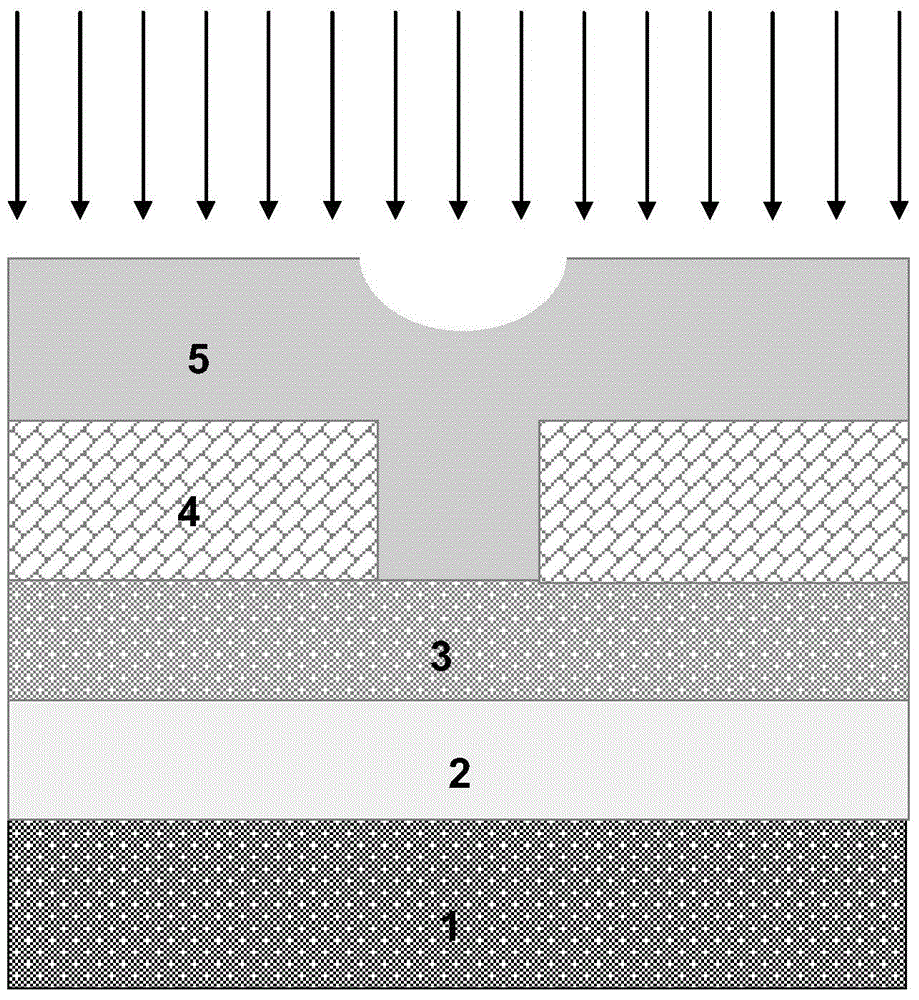
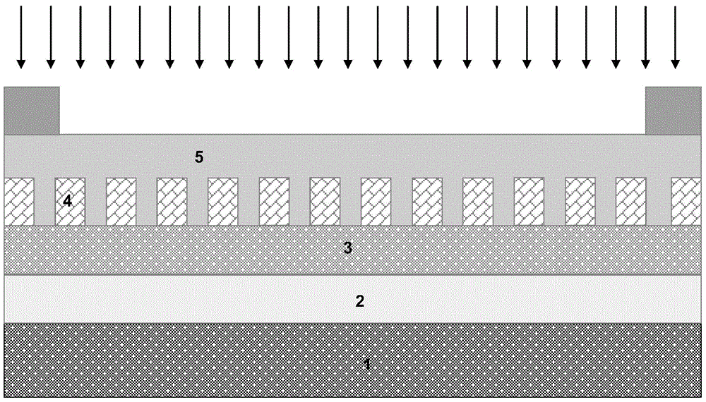
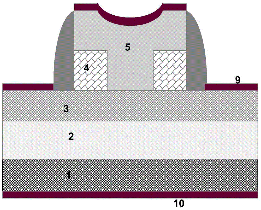
[0024] The compensation method for increasing the direct current amplification factor caused by the thinning of the silicon germanium edge of the present invention is mainly used in the manufacturing process of the emitter area, and the manufacturing process of the collector area and the base area is the same as the commonly used manufacturing process, such as Figure 4 shown. The collector region is manufactured by growing a low N-doped epitaxial layer 2 on a heavily doped N-type silicon substrate 1, with a thickness between 1.0 and 5.0 microns and a doping concentration of 10 15 ~10 17 cm -3 . The manufacture of the base area is to grow a silicon-germanium epitaxial layer 3 on the N-type epitaxial layer 2. The silicon-germanium epitaxial layer 3 is divided into three layers: a silicon buffer layer, a silicon-germanium layer, and a silicon cap layer. Among them, the silicon-germanium layer has a highly doped doped boron and the silicon cap layer has low doped boron. The t...


PUM


Abstract

The invention discloses a compensation method for increase of amplification times of direct current caused by thinning of a germanium-silicon edge. A germanium-silicon layer is formed on an epitaxial layer which is formed on a silicon substrate, a medium film is deposited on the germanium-silicon layer, and an emitter window is formed by etching the medium film to deposit emitter polysilicon. The compensation method includes following steps: performing ion implantation for the first time; plating a layer of negative optical glue, performing chip edge exposure of 8-12mm, removing photoresistance in the middle of a chip by development; and performing ion implantation for the second time. The photoresistance in the middle of the chip is removed by adopting chip edge exposure development, and an edge is covered by the photoresistance, so that the second ion implantation cannot enter the edge, doping concentration of the edge emitter polysilicon is lowered, base diffusion current increases, and ascending of collector current can be effectively compensated; and distribution of in-plane direct current amplification times of a whole single crystal silicon piece is tighter. The compensation method for increase of amplification times of direct current caused by thinning of the germanium-silicon edge is simple in process and remarkably improved in product yield.

Description

technical field [0001] The invention relates to the field of semiconductor integrated circuits, in particular to a method for compensating the increase in collector current caused by edge thinning when germanium and silicon are grown on a non-patterned optical sheet in the manufacturing process of germanium-silicon heterojunction bipolar triode power devices The method of multiplying the dc current method caused by it. Background technique [0002] For radio frequency applications in the 1G Hz range, germanium-silicon heterojunction bipolar transistor devices generally adopt the method of leading out the collector on the back, that is, low N-doped epitaxial growth is performed on the N-type heavily doped substrate to form the collector region. Its advantage is that the process is simple, and the mask layer can be reduced by half compared with the traditional process. The disadvantage is that when silicon germanium is grown on the optical wafer, the thickness of the silicon g...

Claims


Application Information

Patent Timeline
Patent Type & Authority Patents(China)
IPC IPC(8): H01L21/331
Inventor 周正良李昊苏波
Owner SHANGHAI HUAHONG GRACE SEMICON MFG CORP
Why Eureka
Try Eureka