Bi-material railing nanowire tunneling field effect device and manufacturing method thereof

A tunneling field effect, nanowire technology, applied in the direction of semiconductor/solid-state device manufacturing, semiconductor devices, electrical components, etc., can solve the problems of increasing the complexity of the device structure, increasing the cost of the device process, and reducing off-state leakage current, The effect of improving the switching current ratio

Active Publication Date: 2013-03-06
PEKING UNIV SHENZHEN GRADUATE SCHOOL
View PDF5 Cites 4 Cited by
  • Summary
  • Abstract
  • Description
  • Claims
  • Application Information

AI Technical Summary

Problems solved by technology

Its disadvantages are: the dual-gate MOS transistor does not reduce the sub-threshold slope when the device is in operation, thereby increasing the device speed and reducing static power consumption, but by applying dynamic and multi-threshold voltage control, the main gate and auxiliary gate Different bias voltages are used, and the

Method used


Image

  • Bi-material railing nanowire tunneling field effect device and manufacturing method thereof
  • Bi-material railing nanowire tunneling field effect device and manufacturing method thereof
  • Bi-material railing nanowire tunneling field effect device and manufacturing method thereof

Examples


Embodiment Construction

[0040] The present invention will be described in further detail below in conjunction with accompanying drawing:

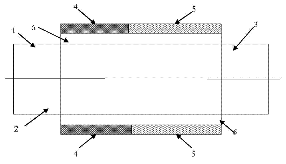
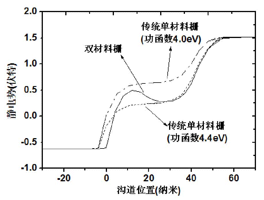
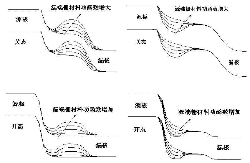
[0041] see figure 1As shown, in this embodiment, the center of the dual-material gate nanowire tunneling field effect device is a channel 2, and the two ends of the channel 2 are respectively provided with a source region 1 and a drain region 3, and the periphery of the channel 2 is sequentially covered. Silicon oxide 6 and gate electrode 4 and gate electrode 5 are provided.

[0042] In this embodiment, the gate electrode 4 and the gate electrode 5 are composed of two metal materials with different work functions. The work function of the material work function of the gate electrode 4 close to the source region 1 is smaller than the work function of the material work function of the gate electrode 5 close to the drain region 3; the work function of the gate electrode 4 close to the source region is 4.0 eV, and the work function of the gate electrode 5 close to th...


PUM

PropertyMeasurementUnit
Work functionaaaaaaaaaa
Thicknessaaaaaaaaaa

Abstract

The invention relates to a bi-material railing nanowire tunneling field effect device and a manufacturing method thereof. According to the bi-material railing nanowire tunneling field effect device, a channel is arranged at the center, and a source region and a drain region are respectively arranged at two ends, and an oxide and a gate electrode are covered at the periphery of the channel in sequence. The manufacturing method comprises the steps: SF6 etching a silicon column on a silicon wafer by using a round silicon nitride hard mask; conducting high-temperature oxidation, corroding and reducing the size of the silicon column to be a set diameter value of 6nm-30nm with HF aqueous solution, and conducting high-temperature oxidation to form a silicon column coated by an oxidation layer with set thickness; completing the preparation of a bi-material railing structure by adopting deposition and photoetching technology; and injecting boron and phosphorus of 1*10<20>cm<-2>/10keV and 5*10<18>cm<-2>/10keV at 120-150 DEG C respectively, and annealing at 900 DEG C/10s-1100 DEG C/10s to prepare the source region and the drain region; completing preparation of a metal electrode by CMOS (Complementary Metal-Oxide-Semiconductor) process; and manufacturing the bi-material railing nanowire tunneling field effect device.

Description

technical field [0001] The invention relates to the field of semiconductor integrated circuit application devices, in particular to a double-material gate nanowire tunneling field effect device and a manufacturing method thereof. Background technique [0002] In recent years, with the continuous shrinking of device size, traditional metal oxide semiconductor field effect devices have encountered bottlenecks such as short channel effects, and further development has been limited. In order to improve the overall performance of devices, researchers have proposed a variety of new devices based on different working principles. Among them, tunneling field effect devices have attracted much attention because of their excellent subthreshold characteristics and very low leakage current. In order to make better use of the performance advantages of tunneling devices, the tunneling mechanism is applied to different device structures, and the characteristics of the new device structure a...

Claims


Application Information

Patent Timeline
IPC IPC(8): H01L29/78H01L29/43H01L21/336H01L21/28
Inventor 何进张爱喜梅金河杜彩霞张立宁叶韵
Owner PEKING UNIV SHENZHEN GRADUATE SCHOOL
Why Eureka
Try Eureka