Absolute pressure transducer chip and production method thereof

A sensor chip, absolute pressure technology, applied in the fluid pressure measurement using capacitance change, manufacturing microstructure devices, decorative arts, etc., can solve the problems of low sensitivity, high cost, poor compatibility, etc., to achieve good compatibility and reliability. High, high-sensitivity effects

Active Publication Date: 2013-03-13
SHENZHEN INST OF ADVANCED TECH
View PDF5 Cites 32 Cited by
  • Summary
  • Abstract
  • Description
  • Claims
  • Application Information

AI Technical Summary

Problems solved by technology

First of all, traditional silicon piezoresistive pressure sensors use diffusion or ion implantation methods to form sensitive resistors, which are very sensitive to temperature and have relatively low sensitivity, which cannot be applied to occasions that require higher sensor sta

Method used


Image

  • Absolute pressure transducer chip and production method thereof
  • Absolute pressure transducer chip and production method thereof
  • Absolute pressure transducer chip and production method thereof

Examples


Embodiment Construction

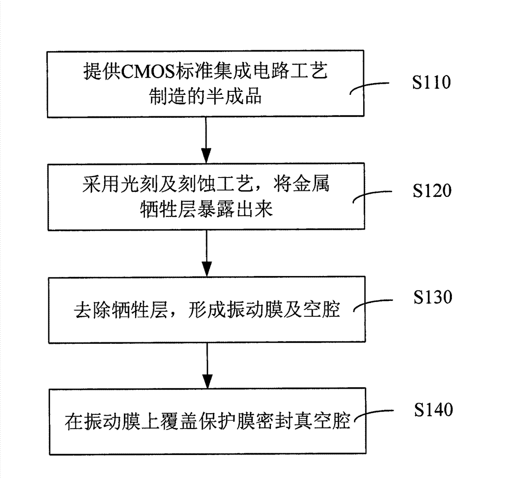
[0028] The absolute pressure sensor chip and its manufacturing method will be described in detail below in conjunction with specific embodiments.

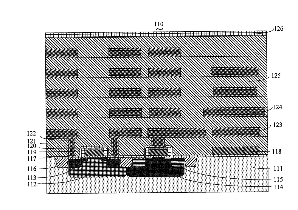
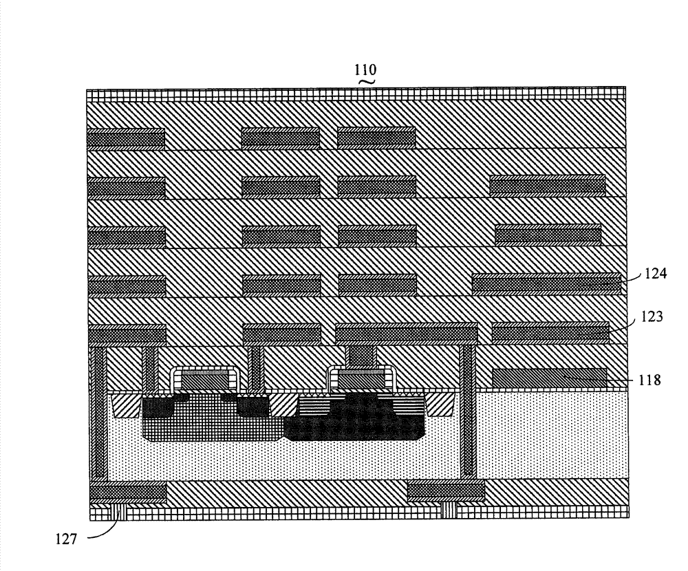
[0029] Please refer to Figure 6 , the absolute pressure sensor chip 100 of this embodiment includes a doped silicon substrate 111 . To produce an integrated circuit chip based on a standard CMOS process, this embodiment is illustrated by using a 1-layer polysilicon 5-layer metal (1P5M) standard CMOS process as an example.

[0030] The designed pattern of the polysilicon layer 118 (as a floating gate electrode) is covered with a conductive vibrating film 130 , and the vibrating film 130 is covered with a protective film 150 to seal the corrosion hole 129 on the vibrating film 130 . The protective film 150 is a polymer film, such as parylene. The protective film 150 closes the vibrating film 130 to form a cavity 140 . The protection film 150 also covers other areas of the chip.

[0031] The backside of the doped silicon substrat...


PUM


Abstract

The invention relates to an absolute pressure transducer chip which comprises an absolute pressure transducer integrated on a complementary metal-oxide-semiconductor transistor (CMOS) chip. The absolute pressure transducer comprises a pressure sensitive unit, the pressure sensitive unit comprises a field-effect tube and a vibrating membrane, the field-effect tube comprises a floating gate, the vibrating membrane is provided with polycrystalline silicon or metal materials serving as grids in inserting mode and is used for inducing absolute pressure change, the floating gate is embedded in a dielectric layer of the CMOS chip, and a cavity is formed on the vibrating membrane and sealed. In the absolute pressure transducer chip, a sacrificial layer and the electric conductive vibrating membrane are manufactured on a metal electric conductive layer of an integrated circuit formed by aid of the CMOS standard manufacture process, and finally a pressure transducer micro-unit is manufactured, the existing CMOS process is not changed, and the absolute pressure transducer chip is good in compatibility. In addition, the invention further relates to a production method of the absolute pressure transducer chip.

Description

technical field [0001] The invention relates to the field of silicon micromechanical sensors, in particular to an absolute pressure sensor chip and a manufacturing method thereof. Background technique [0002] The piezoresistive effect was first discovered by C.S.Smith in 1954, and the piezoresistive pressure sensor is a microsensor designed and processed according to this mechanism. A typical piezoresistive pressure sensor structure is made into a planar thin film by electrochemical or selective doping, anisotropic etching and other processing technologies. The original pressure sensor uses a metal diaphragm as the sensitive element, and silicon strain resistance strips are arranged on it. The successful application of Micro Electro Mechanical Systems (MEMS) technology has prompted people to use the good mechanical properties of silicon to make miniature sensors and actuators. Metal thin films are replaced by single crystal silicon materials, and strain resistance strips a...

Claims


Application Information

Patent Timeline
IPC IPC(8): G01L9/12B81C1/00
Inventor 俞挺彭本贤于峰崎
Owner SHENZHEN INST OF ADVANCED TECH
Why Eureka
Try Eureka