

Processing method for single-cut corrosion slices of monocrystalline silicon wafer
A processing method and technology for corroding sheets, which are applied in chemical instruments and methods, crystal growth, post-processing details, etc., can solve the problems that the corroded sheets are difficult to meet customer requirements, there are line marks on the surface, and the geometric parameters are large, so as to eliminate the need for pouring Corner to grinding, reduced debris rate, uniform response effect
- Summary
- Abstract
- Description
- Claims
- Application Information
AI Technical Summary
Problems solved by technology
Method used
Image

Examples
Embodiment 1
[0026] Example 1: A 5-inch zone melt-doped P oriented silicon wafer with a resistivity of 0.0034±12%Ω.㎝ and a thickness of 203 μm. Take the following process:
[0027] 1) Control the removal amount on both sides of the silicon wafer: 20±2μm.
[0028] 2) According to the product specifications of the silicon wafer, the acid etching solution is prepared according to the concentration percentage of the following components: HF: HNO 3 :CH 3 COOH=9.03%: 39.9%: 23.1%, and the rest is deionized water.
[0029] 3) Add ammonia water as an additive to the acid corrosion solution, and the ammonia water is 2% of the total amount of the acid corrosion solution.
[0030] 4) The surface gloss of the corroded silicon wafer is controlled at 3Gs.
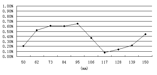
[0031] 5) During the acid corrosion process, ten different positions were selected to blow nitrogen gas into the acid corrosion liquid tank within the range of 50-150 mm of nitrogen gas position, and the comparison of the results is shown in fig...
Embodiment 2
[0036] Example 2: A 5-inch zone melt-doped P oriented silicon wafer with a resistivity of 0.0034±12%Ω.㎝ and a thickness of 203 μm. The process steps are as follows:
[0037] 1) Control the removal amount on both sides of the silicon wafer: 20±2μm.
[0038] 2) According to the product specifications of the silicon wafer, the acid etching solution is prepared according to the concentration percentage of the following components: HF: HNO 3 :CH 3 COOH=9.03%: 39.9%: 23.1%, and the rest is deionized water.
[0039] 3) Add ammonia water as an additive to the acid corrosion solution, and the ammonia water is 2% of the total amount of the acid corrosion solution.
[0040] 4) The surface gloss of the corroded silicon wafer is controlled at 3Gs.
[0041] 5) Select an appropriate process for etching: the temperature of the acid etching solution is kept at 35°C; the rotation rate is 50rpm, and the revolution rate is 10rpm; the circulation volume of the acid etching solution is 300L; th...
PUM
| Property | Measurement | Unit |
|---|---|---|
| Thickness | aaaaa | aaaaa |
Abstract
Description
Claims
Application Information