Method for preparing bismuth, antimony and telluride base thermoelectric film

A thermoelectric thin film, bismuth antimony tellurium technology, applied in the manufacture/processing of thermoelectric devices, vacuum evaporation plating, coating, etc., can solve the problems of easy side effects, low material utilization rate, and high requirements for reaction conditions, and achieve good Adhesion and repeatability, optimization of thermoelectric performance, effect of high ion energy

Active Publication Date: 2013-04-24
SHENZHEN UNIV
View PDF3 Cites 20 Cited by
  • Summary
  • Abstract
  • Description
  • Claims
  • Application Information

AI Technical Summary

Problems solved by technology

In the existing reports, the most commonly used methods for preparing thermoelectric thin films are evaporation and electrochemical deposition. The thin films prepared by the evaporation method have a high power factor, but the thin film prepared by the evaporation method has poor adhesion and the material utilization The efficiency is low, which is a big waste and high cost for rare earth metals, and is not suitable for large-scale production of thermoelectric thin films; the electrochemical deposition method is conducive to reducing the preparation cost due to its simple preparation and low cost, but due to the thin film prepared under non-vacuum conditions , has higher requirements on reaction conditions, is prone to side effects, and is difficult to obtain high-quality films
The sputtering method is one of the most widely used methods for preparing thin films in industrial production. Whether it can prepare high-performance thermoelectric thin films has attracted the attention of many people. In the existing reports, magnetron sputtering and radio frequency sputtering methods are used to prepare The thin film has good adhesion, the preparation method is simple, and the material utilization rate is high. However, because Te with high saturated vapor pressure and Bi with low melting point are difficult to be well controlled in the sputtering process, the thin film elements prepared by alloy target The atomic ratio is different from that of the target, and the uniformity of the film is poor, making it difficult to obtain a high-performance thermoelectric film

Method used


Image

  • Method for preparing bismuth, antimony and telluride base thermoelectric film
  • Method for preparing bismuth, antimony and telluride base thermoelectric film
  • Method for preparing bismuth, antimony and telluride base thermoelectric film

Examples


Embodiment 1

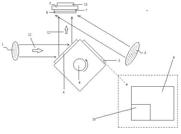
[0031] see figure 1 , which is the ion beam sputtering deposited Bi in the preparation method of bismuth antimony tellurium based thermoelectric thin film of the present invention 2-x Sb x Te 3 Schematic of a thermoelectric thin film. For ease of understanding, first the figure 1 The reference numbers in are explained as follows:

[0032] 1 main sputtering ion source; 2 insulating substrate; 3 auxiliary sputtering ion source; 4 Bi / Te binary composite target; 5 Sb / Te binary composite target; Te alloy film; 8 Sb / Te alloy film; 9 Te high-purity target; 10 Bi or Sb high-purity target; 11 ion beam; 12 sputtering atoms; 13 heating source.

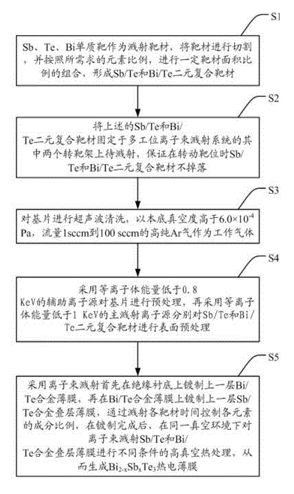
[0033] The Sb, Bi and Te targets with a purity of 99.99% are cut reasonably, and the targets are compounded according to the area ratio of the target as Sb:Te=1:3.5, Bi:Te=1:3 to form a binary Composite target, two binary composite targets of Sb / Te and Bi / Te are respectively fixed on the target frame of two stations; BK7 optical glass is us...

Embodiment 2

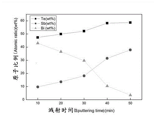
[0037] The difference from Example 1 is that the annealing time of the thermoelectric thin film is changed to 1H, 3H, 4H. Image 6 The sputtering time is 30 min for both BiTe / SbTe. Thin film thermoelectric performance characteristic curve with annealing time of 1H~4H.

Embodiment 3

[0039] The difference from Example 1 is that the annealing temperature of the thermoelectric thin film was changed to 150°C, 200°C, 250°C and 350°C. Figure 7 The thermoelectric performance characteristic curves of BiTe / SbTe films with the sputtering time of 30 min and the annealing temperature of 150°C~350°C.


PUM

PropertyMeasurementUnit
thermoelectric figure of meritaaaaaaaaaa

Abstract

The invention discloses a method for preparing a bismuth, antimony and telluride base thermoelectric film and particularly relates to a Bi[2-x]SbxTe3 base thermoelectric film. In the Bi[2-x]SbxTe3, x is not less than 0.1 and not more than 2.0. According to the method, the ion-beam sputtering depositing method is adopted, two binary complex targets which are Sb/Te and Bi/Te are used as sputtering target materials, the area proportions of the two target materials and the ion-beam sputtering parameters are controlled, and the high-temperature in situ heat treatment is carried out in the same vacuum environment to prepare the Bi[2-x]SbxTe3 thermoelectric film. The method has the advantages of simple process, good repeatability and high utilization rate of raw materials. Due to the adoption of the method, the high-precision controllable doping of elements of the Bi[2-x]SbxTe3 thermoelectric film can be realized, the structure of the Bi[2-x]SbxTe3 thermoelectric film can be optimized effectively, and the thermoelectric properties can be improved.

Description

technical field [0001] The invention relates to the field of thermoelectric functional materials, in particular to a method for preparing a high-performance bismuth-antimony-tellurium-based thermoelectric thin film. Background technique [0002] With the increasingly serious energy crisis, it is urgent to actively promote and promote the use of clean renewable energy, especially the combination of new technology development and industrialization investment in renewable energy to reduce the cost of renewable energy utilization. Thermoelectric devices can realize mutual conversion between thermal energy and electric energy, and are green and environmentally friendly energy devices with a wide range of applications. Semiconductor generators and refrigerators made of semiconductor thermoelectric power generation modules can generate electricity as long as there is a temperature difference, and can be used for cooling when supplying power. They work without noise and pollution, a...

Claims


Application Information

Patent Timeline
Patent Type & Authority Applications(China)
IPC IPC(8): C23C14/06C23C14/34H01L35/34
Inventor 范平郑壮豪梁广兴张东平罗景庭
Owner SHENZHEN UNIV
Why Eureka
Try Eureka