Method of improving light current of silicon thin film solar cell

A solar cell, silicon thin film technology, applied in circuits, electrical components, sustainable manufacturing/processing, etc., can solve the problems of carrier surface recombination, difficult control, complex process, etc., to improve photocurrent, low cost, flexible matching effect

Inactive Publication Date: 2013-05-08
CHINA UNIV OF GEOSCIENCES (BEIJING)
View PDF3 Cites 7 Cited by
  • Summary
  • Abstract
  • Description
  • Claims
  • Application Information

AI Technical Summary

Problems solved by technology

[0003] In order to solve the shortcomings of the current silicon thin film solar cell light trapping technology, the present invention provides a new type of copper nanoparticle surface plasmon light trapping technology. The problem of complex process and difficult control is brought about; at the same time, it also solves the problem of carrier surface recombinat

Method used


Image

  • Method of improving light current of silicon thin film solar cell

Examples


Embodiment Construction

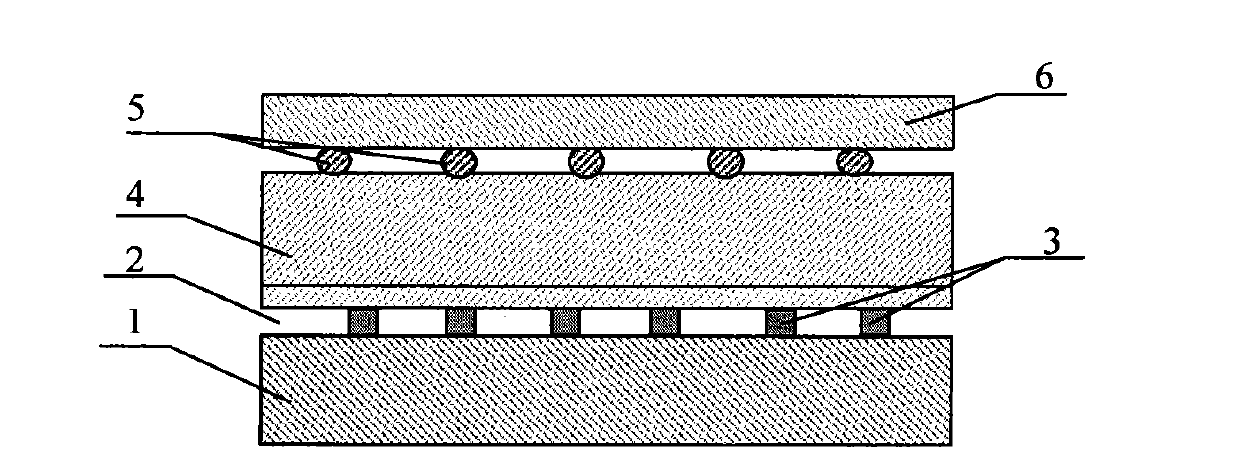
[0014] Such as figure 1 , using transparent conductive glass (1) as the substrate, depositing the copper island film in the magnetron sputtering vacuum chamber, the specific process parameters are as follows: the background vacuum is 5*10 -4 Pa or higher, the purity of the copper target is above 99.99%, the gas is argon with a purity of 99.999%, the deposition pressure is between 0.8Pa-3Pa, the substrate temperature is 150°C-200°C, and the deposition time is 10S-30S. The film thickness is 15nm-30nm. In-situ annealing is carried out on the prepared copper island film in the same vacuum chamber, the annealing temperature is maintained at 300°C-400°C, and the annealing time is 1.5-3 hours to form a copper nanoparticle array (2), the size of which is between 15- Between 30nm, its shape can be spherical, ellipsoidal, cylindrical or prismatic, and the particle distance can be increased by prolonging the annealing time as required. Vacuum for 10-20 minutes after annealing to make t...


PUM

PropertyMeasurementUnit
Thicknessaaaaaaaaaa

Abstract

The invention relates to a method of improving light current of a silicon thin film solar cell, and belongs to the photovoltaic technical field. The light trapping technique of a traditional silicon thin film solar cell mainly comprises that a front electrode and a rear electrode adopt a texture structure which often causes the enlarging of the surface recombination of current carriers and the density of the defect mode of an active layer, and meanwhile due to the fact that wet etching is needed, a process is complex and hard to control. In order to solve the mentioned problems, the invention provides a method of using surface plasmon of copper nanoparticles to increase light absorption, the core technique of the method is that magnet control sputtering equipment is used to deposite copper island film inside a vacuum chamber body, then in situ annealing is carried out to form a copper nanoparticle array, and the copper nanoparticle array is arranged close to two electrodes of the solar cell so as to stimulate the surface plasmon. By using the near field enhancement effect and the scattering effect of the surface plasmon, the light current is further improved. The method of improving the light current of the silicon thin film solar cell does not need wet etching, photoetching and other process, and therefore the cost of batteries can be greatly reduced.

Description

technical field [0001] The invention relates to a method for increasing the photoelectric current of a silicon thin-film solar cell, which belongs to the field of photovoltaic technology. Background technique [0002] In the field of photovoltaics, in order to increase the short-circuit current of silicon thin-film solar cells, people often use light trap technology to increase the distance of light in the cell. The current light trapping technology mainly uses the front electrode with a textured structure or the back reflector on the back of the battery. The biggest feature of this technology is that the transparent electrode has a certain texture, so it can play a role in light trapping. However, this technology also has great defects: (1) The texture of the transparent electrode is mostly formed by wet etching, which not only requires strong corrosive acid, but also the process conditions are not easy to control; (2) This texture Or the density of defect states in the ac...

Claims


Application Information

Patent Timeline
IPC IPC(8): H01L31/18
CPCY02P70/521Y02P70/50
Inventor 郝会颖
Owner CHINA UNIV OF GEOSCIENCES (BEIJING)
Why Eureka
Try Eureka