Fully-differential operation transconductance amplifier

A transconductance amplifier, full differential technology, applied in the direction of differential amplifiers, DC-coupled DC amplifiers, etc., can solve the problems of small OTAGBW and large parasitic capacitance of OTA, so as to reduce parasitic capacitance, increase resistance, and increase output resistance. Effect

Inactive Publication Date: 2013-05-08
TSINGHUA UNIV
View PDF4 Cites 22 Cited by
  • Summary
  • Abstract
  • Description
  • Claims
  • Application Information

AI Technical Summary

Problems solved by technology

[0014] In high-speed analog circuit design, the size of the MOS tube is relatively large, C p1 size relative to C L It cannot be ignored, resulting in a large parasitic capacitance of the telescopic cascode structure OTA, resulting in a small GBW of the OTA

Method used


Image

  • Fully-differential operation transconductance amplifier
  • Fully-differential operation transconductance amplifier
  • Fully-differential operation transconductance amplifier

Examples


Embodiment Construction

[0041] In order to make the object, technical solution and advantages of the present invention clearer, the embodiments of the present invention will be further described in detail below in conjunction with the accompanying drawings.

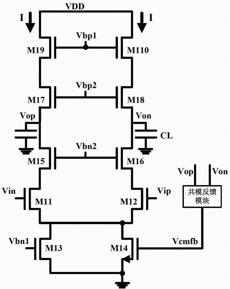
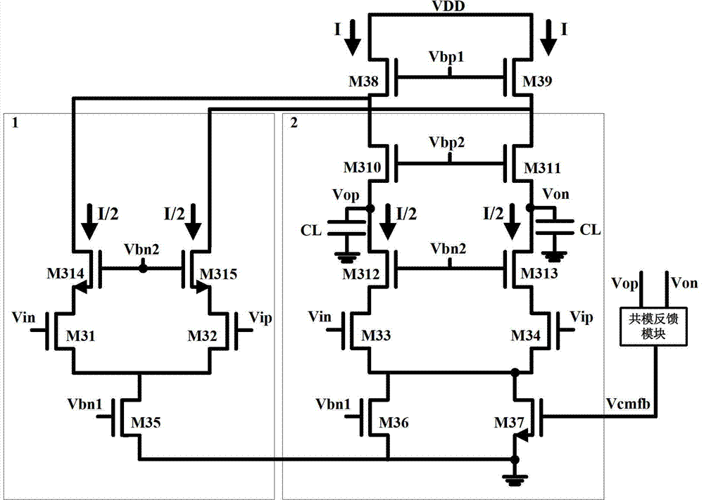
[0042] figure 2 It is a circuit diagram of a fully-differential operational transconductance amplifier (fully-differential OTA) in the first preferred embodiment of the present invention. The fully differential operational transconductance amplifier provided by the embodiment of the present invention can not only improve the gain, but also improve the GBW of the OTA. The input is a differential signal Vin and Vip, and the output is a differential signal Von and Vop. The fully differential operational transconductance amplifier has a first branch 1 and a second branch 2 .

[0043] The first branch 1 receives differential input signals Vin and Vip, including N-channel metal oxide semiconductor NMOS transistors M31, NMOS transistors M32, NMOS tr...


PUM


Abstract

The invention discloses a fully-differential operation transconductance amplifier which is provided with a first branch path and a second branch path. The first branch path receives differential input signals Vin and Vip and comprises an N-channel metal oxide semiconductor (NMOS) tube (M31), an NMOS tube (M32), an NMOS tube (M35), an NMOS tube (M314) and an NMOS tube (M315), and the second branch path is a sleeve type common source and common grid structure, receives the differential input signals Vin and Vip, outputs differential output signals Von and Vop, and comprises a P-channel metal oxide semiconductor (PMOS) tube (M38) and a PMOS tube (M39). Source electrodes of the PMOS tube (M38) and the PMOS tube (M39) are connected on a power source VDD, grid electrodes of the PMOS tube (M38) and the PMOS tube (M39) are connected into bias voltage Vbp1, a drain electrode of the PMOS tube (M38) is connected with a drain electrode of the NMOS tube (M314), and a drain electrode of the PMOS tube (M39) is connected with a drain electrode of the NMOS tube (M315).

Description

technical field [0001] The invention relates to the technical field of circuit development, in particular to a fully differential operational transconductance amplifier. Background technique [0002] With the development of CMOS technology, the power supply voltage and transistor intrinsic gain are gradually reduced. For discrete-time signal processing circuits based on switched capacitor circuits, one of the main bottlenecks in performance improvement is high-performance operational transconductance amplifiers (OTA) . The most important indicator of OTA design is the voltage gain (A V ) and gain-bandwidth product (GBW). where voltage gain A V is the transconductance (G m ) and output resistance (R O ), expressed as: A V =G m R O , the gain-bandwidth product GBW is the transconductance (G m ) with the output capacitor (C O ) ratio, expressed as: GBW=G m / C O . There are various existing OTA structures, and the single-stage OTA mainly includes telescopic cascode ...

Claims


Application Information

Patent Timeline
Patent Type & Authority Applications(China)
IPC IPC(8): H03F3/45
Inventor 李福乐李玮韬杨昌宜王志华
Owner TSINGHUA UNIV
Why Eureka
Try Eureka