

A high-speed bump electroplating method for copper interconnects
A copper interconnect and bump technology, applied in circuits, electrolytic processes, electrolytic components, etc., can solve the problems of reliability and uniformity that have not been industrialized, and achieve easy operation and maintenance, simple formula, and fast copper deposition. Effect
- Summary
- Abstract
- Description
- Claims
- Application Information
AI Technical Summary
Problems solved by technology
Method used
Image

Examples
Embodiment Construction
[0022] The specific embodiments of the present invention will be further described below in conjunction with the accompanying drawings.
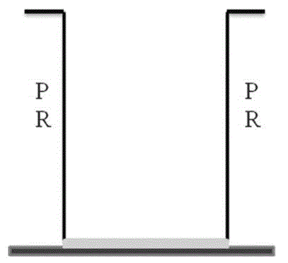
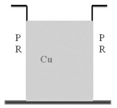
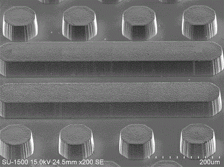
[0023] Such as figure 1 with figure 2 As shown, the high-speed bump electroplating method for copper interconnection provided by the present invention needs to electroplate copper pillars in the electroplating holes shown in the figure, and the power supply used is a special electroplating power supply for PR series circuit boards.
[0024] The method adopts copper sulfonate system electroplating solution to carry out copper bump electroplating, and the electroplating condition is that the current density is 1-25A / dm 2 , temperature 15-35°C, the preferred plating condition is current density 10-16A / dm 2 , temperature 20-30°C.
[0025] The electroplating solution that adopts comprises: the copper methanesulfonate of 160-350g / L and the methanesulfonic acid of 30-180g / L by weight volume ratio, and the chloride ion of 10-80mg / L; This electro...
PUM
| Property | Measurement | Unit |
|---|---|---|
| height | aaaaa | aaaaa |
Abstract
Description
Claims
Application Information