Eureka AIR delivers breakthrough ideas for toughest innovation challenges, trusted by R&D personnel around the world.

Molybdenum plate nickel plating method for silicon power electronic device

A technology for power electronic devices and molybdenum sheets is applied in the field of semiconductor devices, which can solve the problems of poor environmental protection, failure to meet thickness requirements, and restriction on the thickness of nickel-plated nickel layers, and achieves the effects of convenient operation and easy control of the thickness of nickel-plated layers of molybdenum sheets.

Active Publication Date: 2013-06-05
浙江正邦电子股份有限公司
View PDF2 Cites 3 Cited by
  • Summary
  • Abstract
  • Description
  • Claims
  • Application Information

AI Technical Summary

Problems solved by technology

The whole process of nickel plating requires the operator to continuously stir the molybdenum sheet, which is labor intensive and the working environment is poor
In addition, due to the limitation of the nickel content in the heating container and the plating solution, the thickness of the nickel-plated nickel layer is restricted, and often cannot meet the thickness requirements.
In addition, the plating solution must be poured out after one use, which is basically a one-time use, resulting in a large amount of sewage discharge, poor environmental protection, high cost of chemical reagent consumption and sewage treatment

Method used


Image

  • Molybdenum plate nickel plating method for silicon power electronic device

Examples


Embodiment Construction

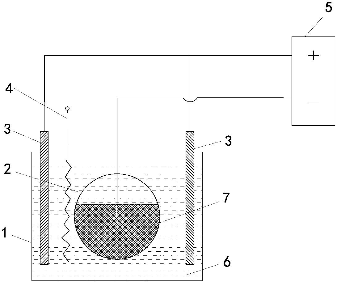
[0009] Description of drawings: electroplating tank 1, drum 2, metal nickel plate 3, electric heating tube 4, electroplating power supply 5, plating solution 6, molybdenum sheet 7.

[0010] Such as figure 1 Shown, a kind of nickel-plating method of molybdenum sheet of silicon power electronic device is that described molybdenum sheet 7 is put into cylinder 2 and is immersed in the plating bath together and is barrel-plated, and nickel sulfate 250g / L, nickel chloride 50g / L are contained in the plating bath. L, boric acid 45g / L and magnesium sulfate 20g / L; the temperature of the plating solution is 40-55°C, the pH value is 8-9, the rotating speed of the drum 2 is 10-15 rpm, and the anode of the electroplating power supply is connected to the electroplated metal nickel plate 3 , the anode current is 80-90A, the cathode is introduced into the drum to contact the molybdenum sheet, and the electroplating time is 40-60 minutes; the molybdenum sheet 7 is nickel-plated once, poured out...


PUM


Abstract

The invention relates to a molybdenum plate nickel plating method for a silicon power electronic device. The method is characterized by comprising the following steps of: placing a molybdenum plate in a cylinder and immersing the molybdenum plate and the cylinder into a plating liquid for barrel plating, wherein the plating liquid comprises 250g / L of nickel sulfate, 50g / L of nickel chloride, 45g / L of boric acid and 20g / L of magnesium sulfate, the temperature of the plating liquid is 40-55 DEG C, the pH value is 8-9, the rotating speed of the cylinder is 10-15rpm; connecting a plating power supply anode with a metal nickel plate to be plated, wherein the anode current is 80-90A; leading the cathode into the cylinder to be in contact with the molybdenum plate, and plating for 40-60 minutes; after primary nickel plating of the molybdenum plate, pouring the molybdenum plate out of the cylinder and washing with clean water; then, drying, and placing nitrogen introducing furnace alloy conventionally; after annealing, repeatedly performing secondary nickel plating according to the method; and then pouring the molybdenum plate, and washing and drying the molybdenum plate. The thickness of the nickel plating layer of the molybdenum plate is easy to control, the method is convenient to operate, and the plating liquid can be repeatedly used.

Description

technical field [0001] The invention relates to a nickel-plating method for molybdenum sheets of silicon power electronic devices, which belongs to the technical field of semiconductor devices. Background technique [0002] Silicon power electronic devices, such as thyristors, diodes and other devices, use molybdenum sheets as linings. Because the thermal expansion coefficient of the molybdenum sheet is close to that of silicon, and has good electrical and thermal conductivity, the molybdenum sheet is used not only as a supporting sheet to enhance strength, but also as an electrode. The combination of molybdenum sheet and silicon sheet usually has two methods of aluminum sintering bonding and lead-tin enamel welding. Generally, aluminum sintering is used between molybdenum sheet and silicon sheet for high-current tubes with more than 200 amperes. The molybdenum sheet of the tube below the current is combined with the silicon sheet by lead-tin enamel welding. Since the moly...

Claims


Application Information

Patent Timeline
Patent Type & Authority Applications(China)
IPC IPC(8): C25D3/12C25D5/14C25D17/16
Inventor 项卫光朱泽鑫徐伟李有康李晓明
Owner 浙江正邦电子股份有限公司
Why Eureka
Eureka Blog
Learn More