Composite structure based on metamaterials and semiconductor low dimension quantum materials and application thereof

A composite structure and semiconductor technology, applied in optical demodulation, instrumentation, optics, etc., can solve problems such as all-optical switches and all-optical wavelength converters that have not yet been discovered, and achieve broad application range, large extinction ratio, and small response time Effect

Inactive Publication Date: 2013-06-05
HUAZHONG UNIV OF SCI & TECH
View PDF1 Cites 21 Cited by
  • Summary
  • Abstract
  • Description
  • Claims
  • Application Information

AI Technical Summary

Problems solved by technology

[0009] After searching, the inventors of the present application have not found any report on combining metamaterials and semiconductor low-dimensional quantum materials to construct all-optical switches or all-optical wavelength converters

Method used


Image

  • Composite structure based on metamaterials and semiconductor low dimension quantum materials and application thereof
  • Composite structure based on metamaterials and semiconductor low dimension quantum materials and application thereof
  • Composite structure based on metamaterials and semiconductor low dimension quantum materials and application thereof

Examples


Embodiment 1

[0033] Example 1. Composite structure based on metamaterials and semiconductor low-dimensional quantum materials

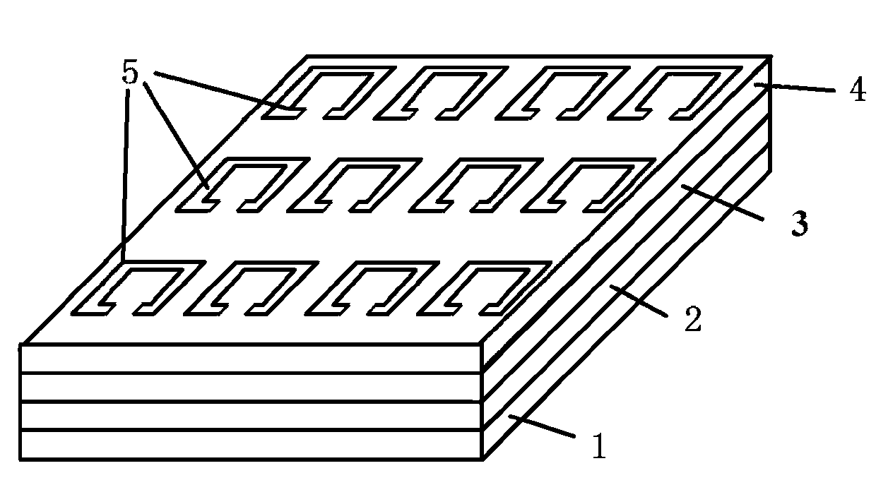
[0034] see figure 1 , which is an embodiment of the composite structure of the present invention based on metamaterials and semiconductor low-dimensional quantum materials, which can be used for all-optical switches and all-optical wavelength conversion.

[0035] The composite structure is composed of substrate 1, buffer layer 2, semiconductor low-dimensional quantum material 3, semiconductor interlayer material 4, and metamaterial 5 arranged from bottom to top ( figure 1 ). Among them: metamaterial 5 is a periodically arranged metal wire array, a periodically arranged metal split resonator ring array or a fishnet structure; and semiconductor low-dimensional quantum material 3 refers to semiconductor quantum wells, quantum wires, and quantum dots. Between the metamaterial 5 and the semiconductor low-dimensional quantum material 3 is a very thin semiconductor i...

Embodiment 2

[0042] Example 2. Preparation of a composite structure based on metamaterials and semiconductor low-dimensional quantum materials

[0043] The following briefly gives a production figure 1 The shown process flow based on the composite structure of metamaterials and semiconductor low-dimensional quantum materials:

[0044] (1) Using metal organic chemical vapor deposition (MOCVD) equipment on the InP substrate to epitaxially grow a 1-1.5-micron thick InP buffer layer and 1-3 cycles of InGaAsP / InP low-dimensional quantum materials from bottom to top ( Well material is In 0.85 Ga 0.15 As 0.65 P 0.35 , thickness of 10 nanometers; barrier region material InP thickness of 11 nanometers), 5 nanometers - 50 nanometers thick InP interlayer material.

[0045] (2) Next, on the InP interlayer material, use an electron beam exposure machine to write the SRR array pattern.

[0046] (3) Deposit gold with a thickness of 30 nanometers using electron beam evaporation equipment.

[0047]...

Embodiment 3

[0050] Example 3. An all-optical switch based on a composite structure of metamaterials and semiconductor low-dimensional quantum materials

[0051] On the basis of the composite structure based on metamaterials and semiconductor low-dimensional quantum materials described in Example 1, adding control light 6 and working light 7 can be used as an all-optical switch, such as Figure 4 shown. Both the control light 6 and the working light 7 are vertically incident from the side of the metamaterial 5 , and they pass through each component of the composite structure in turn, and are transmitted from the side of the substrate 1 . Output light refers to transmitted light.

[0052] The all-optical switch involves two beams of incident light, one of which is the control light 6 and the other is the working light 7; the on or off of the control light 6 determines the on and off state of the output working light 7. The photon energy E1 of the working light 7 is smaller than the photon...


PUM

PropertyMeasurementUnit
thicknessaaaaaaaaaa
lengthaaaaaaaaaa
thicknessaaaaaaaaaa

Abstract

The invention provides a composite structure based on metamaterials and semiconductor low dimension quantum materials. The composite structure based on the metamaterials and the semiconductor low dimension quantum materials is composed of a substrate (1), a buffer layer (2), the semiconductor low dimension quantum materials (3), semiconductor interlayer materials (4) and the metamaterials (5). The metamaterials (5) is in the structure of cycle-assigned metal wire arrays, cycle-assigned metal opening resonance ring arrays or a fishing net. The thickness of the semiconductor interlayer materials (4) is 5 to 50 nanometers. According to the composite structure based on the metamaterials and the semiconductor low dimension quantum materials, a light gain property of the semiconductor low dimension quantum materials and a high speed response property of semiconductor materials to a light signal are simultaneously used, and the composite structure based on the metamaterials and the semiconductor low dimension quantum materials has the dual functions of compensating metamaterial wastage and regulating and controlling metamaterial properties. Under the condition that control light or pump light is additionally arranged, according to the composite structure based on the metamaterials and the semiconductor low dimension quantum materials, the functions of full light opening and closing or full light wavelength conversion can be achieved, and the composite structure based on the metamaterials and the semiconductor low dimension quantum materials has the advantage of being large in extinction ratio.

Description

technical field [0001] The invention relates to the technical field of all-optical signal processing in the field of optical fiber communication, in particular to a composite structure based on metamaterials and semiconductor low-dimensional quantum materials and its application. Background technique [0002] The English name of metamaterial is metamaterial, which has extraordinary electromagnetic properties that natural materials do not have. Although the research on metamaterials has only been carried out for more than ten years, its concept has been expanded from the original, narrow negative refractive index materials to a wider category, including other optical systems, such as photonic crystals, strongly anisotropic materials , nanotransmission lines, chiral materials and supermagnetic materials, etc. It is well known that the permittivity ε and magnetic permeability μ of most natural materials are positive, and the refractive index n (n = ) is also a positive value...

Claims


Application Information

Patent Timeline
Patent Type & Authority Applications(China)
IPC IPC(8): G02B5/00G02F1/017G02F2/00
Inventor 黄黎蓉孙荣
Owner HUAZHONG UNIV OF SCI & TECH
Why Eureka
Try Eureka