Structure of front end of gallium arsenide base monolithic photoelectron integrated receiver and manufacturing method thereof

A receiver front-end, gallium arsenide-based technology, which is applied in the field of front-end structure and production of gallium arsenide-based monolithic optoelectronic integrated receivers, can solve the problems of restricting the bandwidth advantage of distributed amplifiers, so as to improve the success rate of one-time casting, parasitic The effect of small capacitance and small damage

Inactive Publication Date: 2010-06-16
NO 55 INST CHINA ELECTRONIC SCI & TECHNOLOGYGROUP CO LTD
View PDF0 Cites 4 Cited by
  • Summary
  • Abstract
  • Description
  • Claims
  • Application Information

AI Technical Summary

Problems solved by technology

Distributed amplifier gate, drain transmission line characteristic impedance, cut-off frequency, terminal load, etc. determine its main electrical performance, and due to the existence of distribution effects, the transmission line layout affects the above characteristics to a large extent, and there are a large number of transmission line layouts in the current design. Further improvement, which to some extent restricts the full play of the bandwidth advantages of the distributed amplifier

Method used


Image

  • Structure of front end of gallium arsenide base monolithic photoelectron integrated receiver and manufacturing method thereof
  • Structure of front end of gallium arsenide base monolithic photoelectron integrated receiver and manufacturing method thereof
  • Structure of front end of gallium arsenide base monolithic photoelectron integrated receiver and manufacturing method thereof

Examples


Embodiment 1

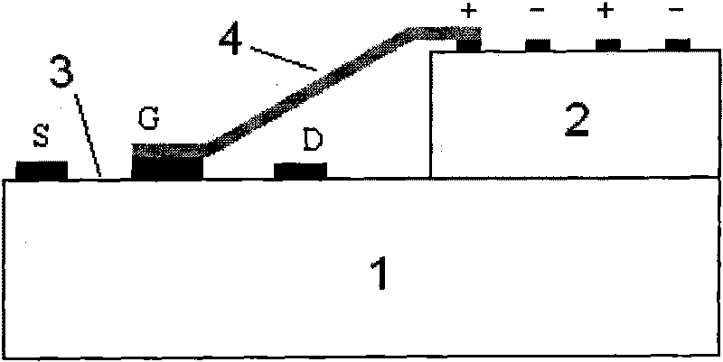
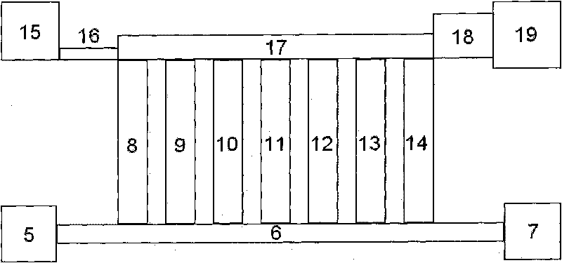
[0021]Embodiment 1: Design the GaAs-based monolithic optoelectronic integrated receiver front end, its structure includes a distributed preamplifier and a photodetector, wherein the length and width of the source electrode 33 of the distributed preamplifier PHEMT device are 10 μm and 50 μm respectively, and the gate The length and width of the electrode 34 are 0.5 μm and 100 μm respectively, and the length and width of the drain 35 are 10 μm and 50 μm respectively; the amplifier adopts 7 common source-common gate structures as the gain unit, the terminal load of the gate transmission line is 7, and the reverse terminal load of the drain transmission line The impedance of 15 is 50Ω, the grid transmission line input microstrip 6 has a width of 10 μm and a length of 1780 μm, the resistance values ​​of resistors 24 and 27 are 15Ω and 148Ω respectively, the capacitance 22 is 2.1pF, and the width and length of microstrip line 20 are 10 μm and 200 μm, respectively. The width and lengt...

Embodiment 2

[0025] Embodiment 2: Design the GaAs-based monolithic optoelectronic integrated receiver front-end, its structure includes a distributed preamplifier and a photodetector, wherein the length and width of the source electrode 33 of the distributed preamplifier PHEMT device are 10 μm and 50 μm, and the gate The pole length and width are 340.5 μm and 100 μm respectively, and the length and width of the drain 35 are 10 μm and 50 μm respectively; the amplifier adopts 7 common source-common gate structures as the gain unit, and the characteristic impedance of the transmission line and the impedance of the terminal load 7 and 15 are both 50Ω , the gate transmission line input microstrip 6 has a width of 10 μm and a length of 1780 μm, the resistance values ​​of the resistors 24 and 27 are 22Ω and 148Ω respectively, the capacitance 22 is 2.1pF, the width and length of the microstrip line 20 are 10 μm and 200 μm respectively, and the width of the microstrip line 23 The width and length of...


PUM


Abstract

The invention discloses a structure of the front end of a gallium arsenide base monolithic photoelectron integrated receiver and a manufacturing method thereof. Aiming at a distributed amplifier adopting cascode structure as a gain unit, the invention provides a method comprising grid transmission line micro-strip straight line layout, a leakage transmission line forward and reverse terminal micro-strip impedance adjustment as well as resistance and a plurality of micro-strip line impedance adjustment in a gain unit, which obtains favourable frequency domain and time domain response; the method combines gallium arsenide PHEMT amplifier technology and MSM photodetector technology, adopts the technology of forming a photodetector table board by reactive ion etching, the technology of successively manufacturing MSM photodetector interdigital electrodes and PHEMT device grid electrodes, and the anti-reflection and passivation medium technology of forming the MSM photodetector by three-time silicon nitride medium deposition. The invention has the advantages that the distributed amplifier has compact layout and favorable combination property, the band width advantage is fully performed, and combination property is favorable; monolithic integration technology is reasonable, gives consideration to the characteristics of both the PHEMT amplifier and the MSM photodetector detector and has high flowing efficiency.

Description

technical field [0001] The present invention relates to a monolithic optoelectronic integrated receiver front-end structure and manufacturing method, in particular to a gallium arsenide pseudo-high electron mobility transistor (PHEMT) amplifier and a metal-semiconductor-metal photodetector (MSM PD) The design and manufacturing process of monolithic integration belongs to the cross field of monolithic microwave integrated circuit and optoelectronic technology. Background technique [0002] Monolithic optoelectronic integration manufactures optoelectronic devices such as lasers and photodetectors and microwave circuits such as preamplifiers and limiting amplifiers on the same substrate (single chip) to minimize the impact of interconnection parasitic parameters on the maximum operating rate of the device. Limitations, and the elimination or reduction of interconnection solder joints is conducive to improving the reliability of integrated devices. The optical receiver front en...

Claims


Application Information

Patent Timeline
Patent Type & Authority Applications(China)
IPC IPC(8): H01L27/144H01L21/8252H04B1/16
Inventor 焦世龙陈堂胜叶玉堂钱峰
Owner NO 55 INST CHINA ELECTRONIC SCI & TECHNOLOGYGROUP CO LTD
Why Eureka
Try Eureka